GS841E18AB-100 View Datasheet(PDF) - Giga Semiconductor
Part Name
Description
Manufacturer
GS841E18AB-100 Datasheet PDF : 21 Pages
| |||
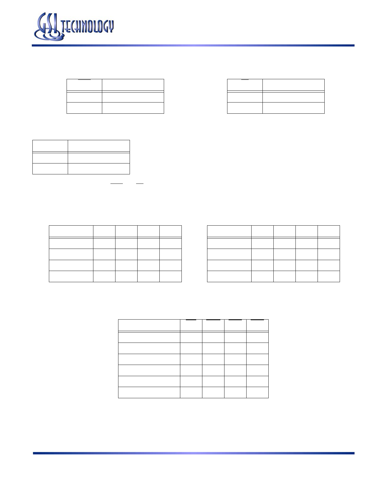
Mode Pin Function
GS841E18AT/B-180/166/150/130/100
LBO
L
H or NC
Power Down Control
Function
Linear Burst
Interleaved Burst
FT
L
H or NC
Function
Flow Through
Pipeline
ZZ
Function
L or NC
Active
H
Standby, IDD = ISB
Note:
There are pull up devices on LBO and FT pins and pull down device on ZZ pin, so those input pins can be unconnected
and the chip will operate in the default states as specified in the above tables.
Linear Burst Sequence
A[1:0] A[1:0] A[1:0] A[1:0]
1st address
00
01
10
11
2nd address
01
10
11
00
3rd address
10
11
00
01
4th address
11
00
01
10
Interleaved Burst Sequence
A[1:0] A[1:0] A[1:0] A[1:0]
1st address
00
01
10
11
2nd address
01
00
11
10
3rd address
10
11
00
01
4th address
11
10
01
00
Byte Write Function
Function
GW BWE BW1
Read
H
H
X
Read
H
L
H
Write all bytes
L
X
X
Write all bytes
H
L
L
Write byte 1
H
L
L
Write byte 2
H
L
H
BW2
X
H
X
L
H
L
Note: H = logic high, L = logic low, NC = no connect
Rev: 1.03 4/2005
7/21
Specifications cited are subject to change without notice. For latest documentation see http://www.gsitechnology.com.
© 2001, GSI Technology
Share Link: 