GS841E18AB-100 View Datasheet(PDF) - Giga Semiconductor
Part Name
Description
Manufacturer
GS841E18AB-100 Datasheet PDF : 21 Pages
| |||
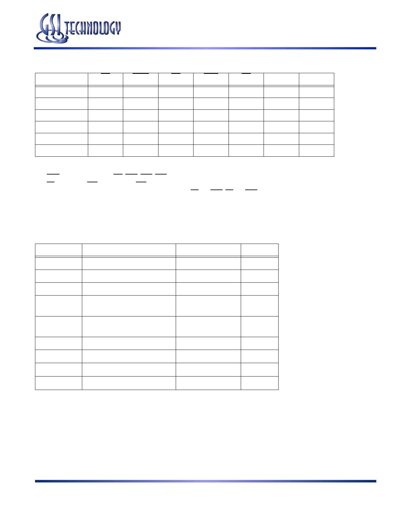
GS841E18AT/B-180/166/150/130/100
Truth Table For Read/Write/Compare/Fill Write Operation
CE
Write
DE
MOE
OE
Match
DQ
Read
L
H
X
X
L
—
Q
Write
L
L
L
X
H
—
D
Compare
L
H
L
L
H
Data Out
D
Fill Write
L
L
H
X
X
—
X
Match Deselect
H
X
X
L
X
High
High Z
Deselect
H
X
X
H
X
High Z
High Z
Notes:
1. X means “don’t care,” H means “logic high,” L means “logic low.”
2. Write is the logic function of GW, BWE, BW1, BW2. See Byte Write Function table for detail.
3. CE is defined as CE1=L, CE2=H and CE3=L
4. All signals are synchronous and are sampled by CLK except OE and MOE. OE and MOE are asynchronous and drive the bus immediately.
)
Absolute Maximum Ratings (Voltage reference to VSS = 0 V)
Symbol
Description
Commerical
Unit
VDD
Supply Voltage
–0.5 to 4.6
V
VDDQ
Output Supply Voltage
–0.5 to VDD
V
VCLK
CLK Input Voltage
–0.5 to 6
V
Vin
Input Voltage
–0.5 to VDD + 0.5
(≤ 4.6 V max. )
V
Vout
Output Voltage
–0.5 to VDD + 0.5
(≤ 4.6 V max. )
V
Iout
Output Current per I/O
+/–20
mA
PD
Power Dissipation
1.5
W
TOPR
Operating Temperature
0 to 70
oC
TSTG
Storage Temperature
–55 to 125
oC
Note:
Permanent damage to the device may occur if the Absolute Maximun Ratings are exceeded. Functional operation should be restricted to the
recommended operation conditions. Exposure to higher than recommended voltages, for an extended period of time, could effect the
performance and reliability of this component.
Rev: 1.03 4/2005
9/21
Specifications cited are subject to change without notice. For latest documentation see http://www.gsitechnology.com.
© 2001, GSI Technology
Share Link: 