LTC6991HS6 View Datasheet(PDF) - Analog Devices
Part Name
Description
Manufacturer
LTC6991HS6 Datasheet PDF : 24 Pages
| |||
LTC6991
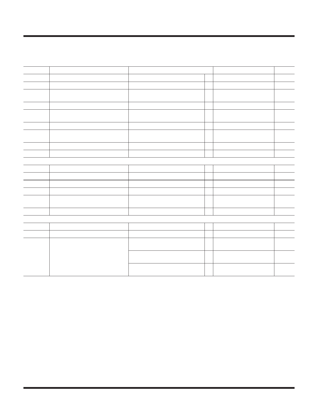
ELECTRICAL CHARACTERISTICS The l denotes the specifications which apply over the full operating
(teNmDIpVe=ra1tutore2r2a1n),geR,SEoTth=er5w0kisteos8p0e0cki,ficRaLtOioADns=a5rke,aCtLTOAAD=
25°C.
= 5pF
Test conditions are V+ =
unless otherwise noted.
2.25V
to
5.5V,
RST
=
0V,
DIVCODE
=
0
to
15
SYMBOL
tOUT
fOUT
∆fOUT
PARAMETER
Output Clock Period
Output Frequency
Frequency Accuracy (Note 4)
CONDITIONS
29.1µHz ≤ fOUT ≤ 977Hz
∆fOUT/∆T
∆fOUT/∆V+
Frequency Drift Over Temperature
Frequency Drift Over Supply
Long-Term Frequency Stability
Period Jitter (Note 10)
BW
Frequency Modulation Bandwidth
tS
Frequency Change Settling Time (Note 9)
Analog Inputs
VSET
∆VSET/∆T
RSET
VDIV
∆VDIV/∆V+
Voltage at SET Pin
VSET Drift Over Temperature
Frequency-Setting Resistor
DIV Pin Voltage
DIV Pin Valid Code Range (Note 5)
DIV Pin Input Current
Power Supply
V+
Operating Supply Voltage Range
Power-On Reset Voltage
IS
Supply Current
V+ = 4.5V to 5.5V
V+ = 2.25V to 4.5V
(Note 11)
NDIV = 1
NDIV = 8
Deviation from Ideal
VDIV/V+ = (DIVCODE + 0.5)/16
RL = ∞, RSET = 50k
RL = ∞, RSET = 100k
RL = ∞, RSET = 800k
V+ = 5.5V
V+ = 2.25V
V+ = 5.5V
V+ = 2.25V
V+ = 5.5V
V+ = 2.25V
MIN
TYP
MAX
UNITS
1.024m
34,360 Seconds
29.1µ
977
Hz
±0.8
±1.5
%
l
±2.2
%
l
±0.005
%/°C
l
0.23
0.55
%/V
l
0.06
0.16
%/V
90
ppm/√kHr
15
7
0.4 • fOUT
1
ppmRMS
ppmRMS
Hz
Cycle
l 0.97
1.00
1.03
l
±75
l 50
800
l
0
V+
l
±1.5
l
±10
V
µV/°C
kΩ
V
%
nA
l 2.25
5.5
V
l
1.95
V
l
135
170
µA
l
105
135
µA
l
100
130
µA
l
80
105
µA
l
65
100
µA
l
55
85
µA
For more information www.linear.com/LTC6991
6991fc
3
Share Link: 