ZXCL330 View Datasheet(PDF) - Zetex => Diodes
Part Name
Description
Manufacturer
ZXCL330 Datasheet PDF : 11 Pages
| |||
ZXCL Series
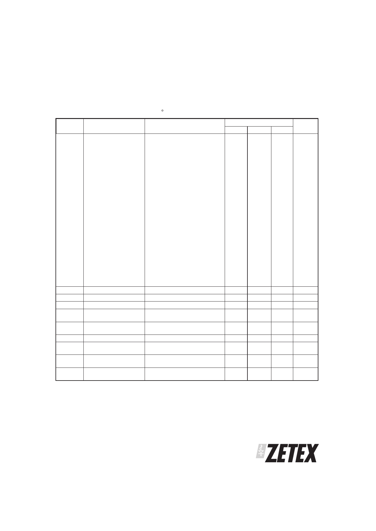
ELECTRICAL CHARACTERISTICS
VIN = VO + 0.5V, all values at TA = 25 C (Unless otherwise stated)
SYMBOL PARAMETER
CONDITIONS
MIN
VDO
Dropout Voltage
Note 3
ZXCL250 / 5213v25
IO=10mA
IO=50mA
IO=100mA
ZXCL260 / 5213v26
IO=10mA
IO=50mA
IO=100mA
ZXCL280 / 5213v28
IO=10mA
IO=50mA
IO=100mA
ZXCL300 / 5213v30
IO=10mA
IO=50mA
IO=100mA
ZXCL330 / 5213v33
IO=10mA
IO=50mA
IO=100mA
ZXCL400 / 5213v40
IO=10mA
IO=50mA
IO=100mA
⌬VLNR
Line Regulation
VIN=(VO+0.5V) to 5.5V, IO=1mA
⌬VLDR
Load Regulation
IO=1mA to 100mA
EN
Output Noise Voltage f=10Hz to 100kHz, CO=10µF,
VENH
Enable pin voltage for
2
normal operation
TA = -40°C
2.2
VENL
Enable pin voltage for
0
output shutdown
VENHS
IEN
Enable pin hysteresis
Enable Pin input
current
VEN=5.5V
IQSD
Shutdown supply
current
VEN=0V
TSD
Thermal Shutdown
125
Temperature
LIMITS
UNITS
TYP
MAX
15
85
mV
163
325
15
mV
85
155
310
15
85
mV
140
280
15
85
mV
140
280
15
85
mV
140
280
15
85
mV
140
280
0.02
0.1 %/V
0.01
0.04 %/mA
50
µV rms
10 V
0.8 V
150
mV
100 nA
1 µA
165 °C
Device testing is performed at TA=25ЊC. Device thermal performance is guaranteed by design.
Note1: Maximum power dissipation is calculated assuming the device is mounted on a PCB measuring 2 inches
square
Note 2: Output Voltage will start to rise when VIN exceeds a value or approximately 1.3V. For normal
operation, VIN (min) > VOUT (nom) + 0.5V.
Note 3: Dropout voltage is defined as the difference between VIN and VO, when VO has dropped 100mV below
its nominal value. Nominal value of VO is defined at VIN=VO+0.5V.
ISSUE 7 - AUGUST 2002
3
Share Link: 