ZXCL400 View Datasheet(PDF) - Zetex => Diodes
Part Name
Description
Manufacturer
ZXCL400 Datasheet PDF : 11 Pages
| |||
ZXCL Series
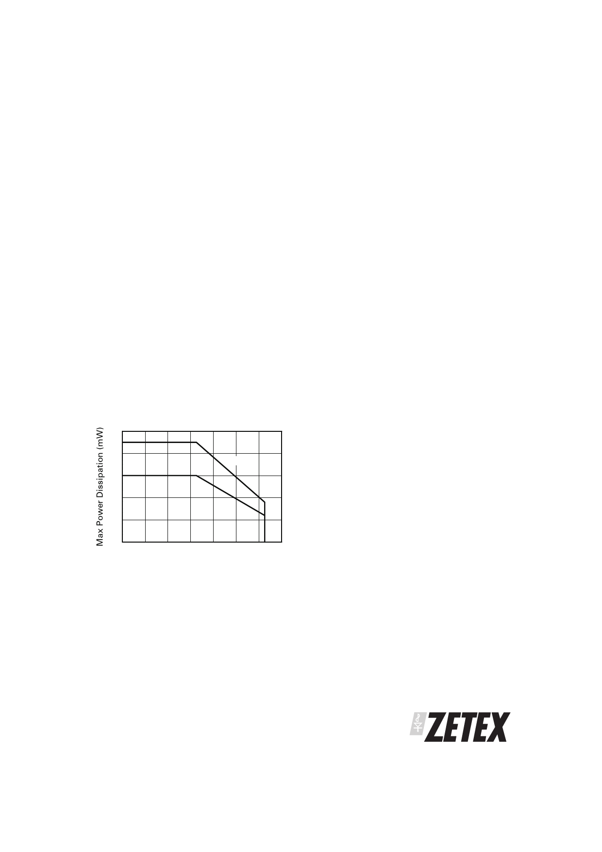
APPLICATIONS INFORMATION (Cont)
Power Dissipation
The maximum allowable power dissipation of the
device for normal operation (Pmax), is a function of the
package junction to ambient thermal resistance (θja),
maximum junction temperature (Tjmax), and ambient
temperature (Tamb), according to the expression:
Pmax = (Tjmax – Tamb) / θja
The maximum output current (Imax) at a given value of
Input voltage (VIN) and output voltage (VOUT) is then
given by
Imax = Pmax / (VIN - VOUT )
The value of θja is strongly dependent upon the type of
PC board used. Using the SC70 package it will range
from approximately 280 °C/W for a multi-layer board to
around 450°C/W for a single sided board. It will range
from 180°C/W to 300°C/W for the SOT23-5 package. To
avoid entering the thermal shutdown state, Tjmax
should be assumed to be 125°C and Imax less than the
over-current limit,(IOLIM). Power derating for the SC70
and SOT23-5 packages is shown in the following
graph.
The dielectric of the ceramic capacitance is an
important consideration for the ZXCL Series operation
over temperature. Zetex recommends minimum
dielectric specification of X7R for the input and output
capacitors. For example a ceramic capacitor with X7R
dielectric will lose 20% of its capacitance over a -40ЊC to
85ЊC temperature range, whereas a capacitor with a
Y5V dielectric loses 80% of its capacitance at -40ЊC and
75% at 85ЊC.
An input capacitor of 1F (ceramic or tantalum) is
recommended to filter supply noise at the device input
and will improve ripple rejection.
The input and output capacitors should be positioned
close to the device, and a ground plane board layout
should be used to minimise the effects of parasitic track
resistance.
Dropout Voltage
The output pass transistor is a large PMOS device,
which acts like a resistor when the regulator enters the
dropout region. The dropout voltage is therefore
proportional to output current as shown in the typical
characteristics.
Ground Current
500
The use of a PMOS device ensures a low value of
ground current under all conditions including dropout,
400
start-up and maximum load.
SOT23
300
Power Supply Rejection and Load Transient Response
200
SC70
100
0
-40 -20
0 20 40 60
Temperature (°C)
Derating Curve
80 100
Capacitor Selection and Regulator Stability
The device is designed to operate with all types of
output capacitor, including tantalum and low ESR
ceramic. For stability over the full operating range from
no load to maximum load, an output capacitor with a
minimum value of 1F is recommended, although this
can be increased without limit to improve load
transient performance. Higher values of output
capacitor will also reduce output noise. Capacitors with
ESR less than 0.5⍀ are recommended for best results.
Line and Load transient response graphs are shown in
the typical characteristics.
These show both the DC and dynamic shift in the
output voltage with step changes of input voltage and
load current, and how this is affected by the output
capacitor.
If improved transient response is required, then an
output capacitor with lower ESR value should be used.
Larger capacitors will reduce over/undershoot, but will
increase the settling time. Best results are obtained
using a ground plane layout to minimise board
parasitics.
ISSUE 7 - AUGUST 2002
9
Share Link: 