INT202TFI2 View Datasheet(PDF) - Power Integrations, Inc
Part Name
Description
Manufacturer
INT202TFI2 Datasheet PDF : 12 Pages
| |||
INT202
General Circuit Operation
The three-phase switched reluctance
motor drive circuit shown in Figure 4
illustrates a typical application for the
INT202/201. The LS IN signal directly
controls MOSFET Q1. The HS IN signal
causes the INT202 to command the
INT201 to turn MOSFET Q2 on or off as
required.
Local bypassing for the low-side driver
is provided by C1. Bootstrap bias for the
high-side driver is provided by D1 and
C2. Slew rate and effects of parasitic
oscillations in the load waveforms are
controlled by resistors R1 and R2.
The inputs are designed to be compatible
with 5 V CMOS logic levels and should
not be connected to V . Normal CMOS
DD
power supply sequencing should be
observed. The order of signal application
should be V , logic signals, and then
DD
HV+. V should be supplied from a
DD
low impedance voltage source.
The length of time that the high-side can
remain on is limited by the size of the
bootstrap capacitor. Applications with
extremely long high-side on times
require special techniques discussed in
AN-10.
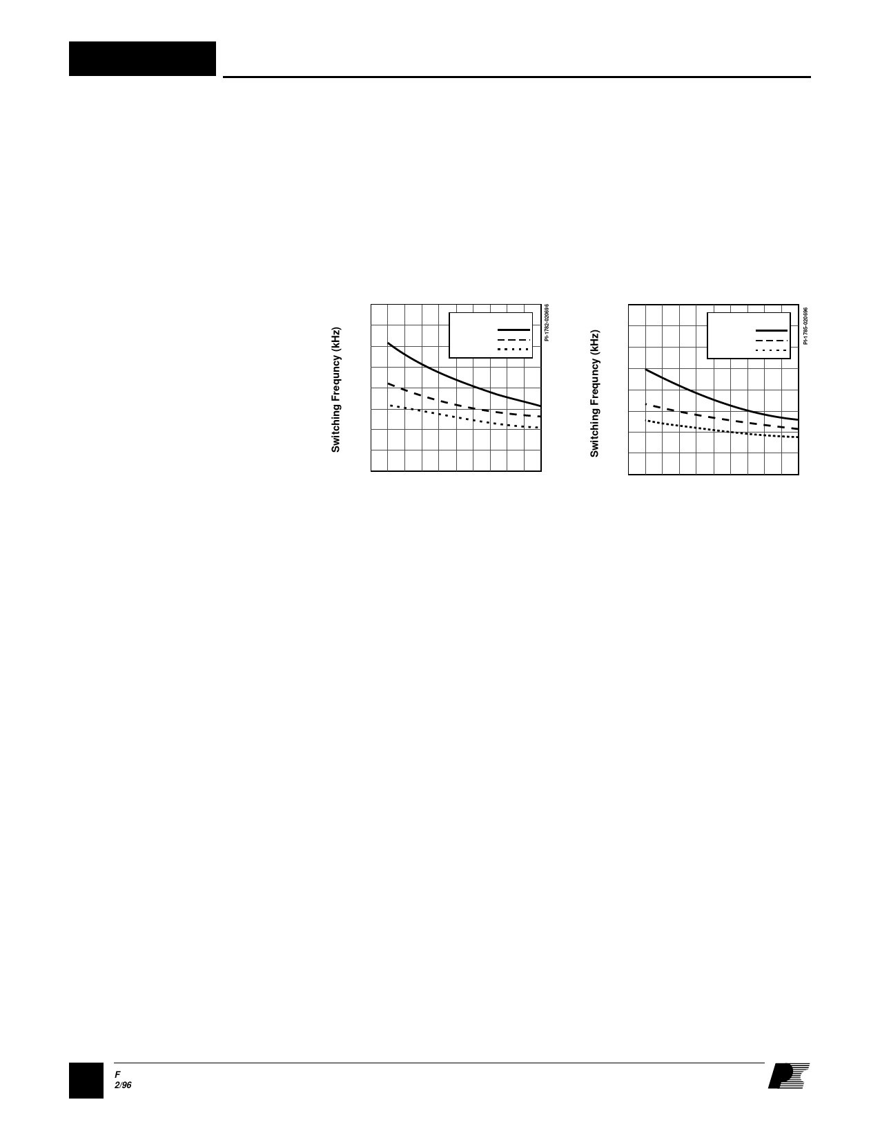
Maximum frequency of operation is
limited by power dissipation due to high-
400
PDIP
VIN = 200 V
300
VIN = 300 V
VIN = 400 V
200
voltage switching, gate charge, and bias
power. Figure 5 indicates the maximum
switching frequency as a function of
input voltage and gate charge. For higher
ambient temperatures, the switching
frequency should be derated linearly.
400
SOIC
VIN = 200 V
300
VIN = 300 V
VIN = 400 V
200
100
100
0
0
100
200
Gate Charge (nC)
0
0
100
200
Gate Charge (nC)
Figure 5. Switching Frequency versus Gate Charge for a) PDIP and b) SOIC.
4F
2/96
Share Link: 