ADM9240 View Datasheet(PDF) - ON Semiconductor
Part Name
Description
Manufacturer
ADM9240 Datasheet PDF : 22 Pages
| |||
ADM9240
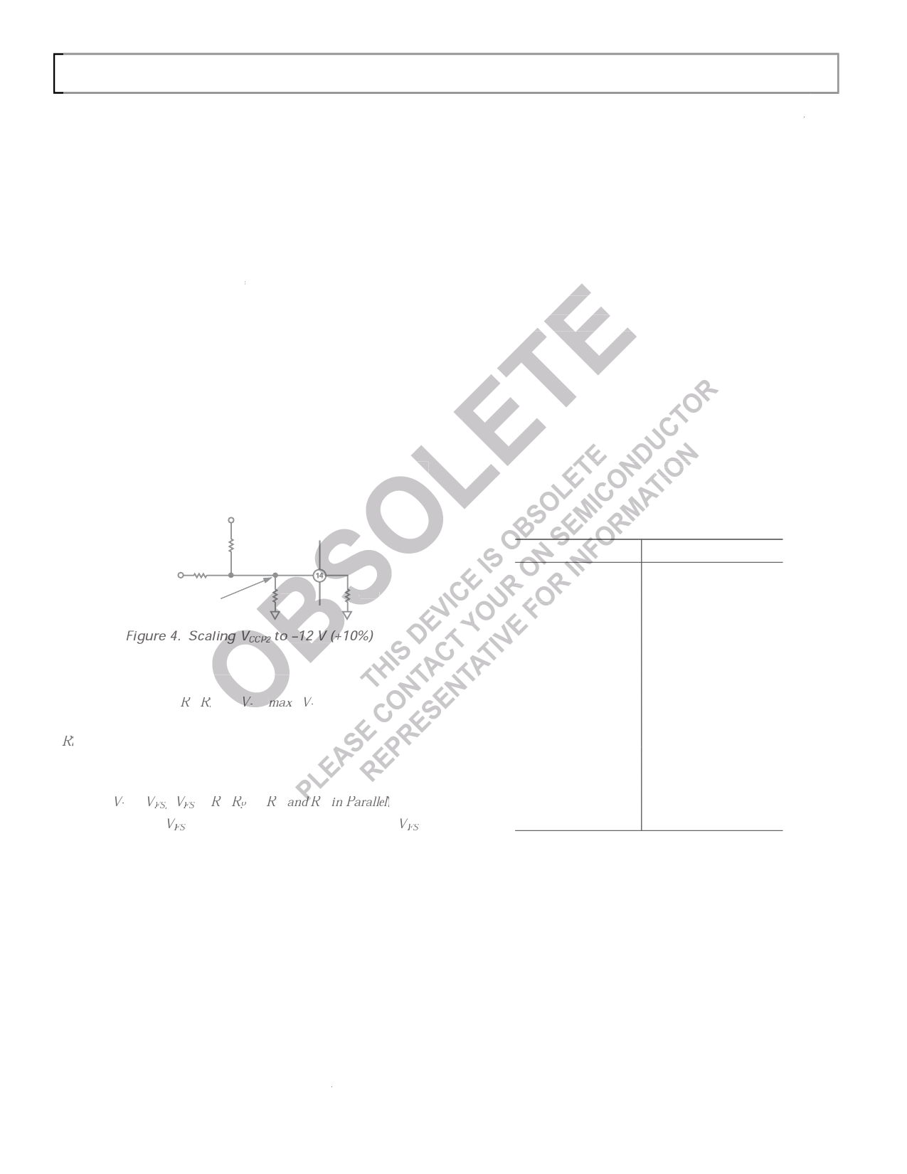
SETTING OTHER INPUT RANGES
If any of the inputs is unused, and there is a requirement for
monitoring another power supply such as –12 V, the input range
of the unused input can easily be scaled and offset to accommo-
date this. For example, if only one processor core voltage is to
be monitored, the unused
another supply voltage.
VCCP
input
can
be
used
to
monitor
If the voltage to be monitored is positive, it is simply a matter of
using an input with a lower full scale than the voltage to be
measured and adding an external input attenuator, but bear in
mind that the input resistance (≈140 kΩ) of the on-chip attenua-
tor will load the external attenuator. This can be accounted for
in the calculation, but the values of the on-chip attenuator resis-
tors are not precise and vary with temperature. Therefore, the
external attenuator should have a much lower output resistance
to minimize the loading. If this is not acceptaibnleP,aarabllueffer ampli-
fier can be used.
If the input voltage range is negative, it must first be converted
to a positive voltage. The simplest way to do this is simply to
attenuate and offset the voltage, as shown in Figure 4, which
shows the
the values
+shVoCwCnP2,
input scaled to
the input range
mmisaezaesruoretoa––1132.5VVi,npwuhti.chUswinilgl
accommodate a +12.5% tolerance on the nominal value.
dt(hReec2r+5eRaVsPes)s,utpwhpheliylieninpacudrteetacosreetshasetehAeinDAtCDh.eC5inVpsuutpbpylythceorDreVsp×onRdP/ingly
3. The on-chip input attenuators will load the external attenua-
tor, as mentioned earlier.
This technique can be applied to any other unused input. By
suitable choice of V+ and the input resistors, a variety of nega-
tive and/or bipolar input ranges can be obtained.
TEMPERATURE MEASUREMENT SYSTEM
The ADM9240 contains an on-chip bandgap temperature sen-
sor. The on-chip ADC performs 9-bit conversions on the output
of this sensor and outputs the temperature data in 9-bit twos
complement format, but only the eight most significant bits are
used for temperature limit comparison. The full 9-bit tempera-
ture data can be obtained by reading the 8 MSBs from the Tem-
perature Value Register (Address 27h) and the LSB from Bit 7
of the Temperature Configuration Register (Address 4Bh).
The format of the temperature data is shown in Table II. Theo-
retically, the temperature sensor and ADC can measure tem-
peratures from –128°C to +127°C with a resolution of 0.5°C,
although temperatures below –40°C and above +125°C are
outside the operating temperature range of the device.
+5V
Table II. Temperature Data Format
CCP
R1
2.7k⍀
–13.2V TO 0V IN
0V TO 3.6V
R2
1k⍀
+VCCP2
R3
39k⍀
Ϸ140k⍀
Figure 4. Scaling VCCP2 to –12 V (+10%)
The resistor ratios are calculated as follows:
R1/R2 = |V–|(max)/V+
(to give zero volts at the input for the most negative value of V–.
R2 has no effect under this condition as the voltage across it is
zero)
and:
(V+ – VFS)/VFS = R2/RP = (R1 and R2 in Parallel)
(to
the
gniovremaavloflutlalg-secValFeSvaotlttahgeeinopf uthtewihnepnutVu–siesdz)e.ro,
where
VFS
is
This is a simple and cheap solution, but the following points
msihnodutlhdabt ethneoitnepdu. t resistance
1. Since the input signal is not inverted, an increase in the mag-
nitude of the –12 V supply (going more negative), will cause
the input voltage to fall and give a lower output code from
the ADC. Conversely, a decrease in the magnitude of the
–12 V supply will cause the ADC code to increase. This
means that the upper and lower limits will be transposed.
2. Since the offset voltage is derived from the +5 V supply,
variations in this supply will affect the ADC code.
Temperature
–128°C
–125°C
–100°C
–75°C
–50°C
–25°C
–0.5°C
0°C
+0.5°C
+10°C
+25°C
+50°C
+75°C
+100°C
+125°C
+127°C
Digital Output
1 0000 0000
1 0000 0110
1 0011 1000
1 0110 1010
1 1001 1100
1 1100 1110
1 1111 1111
0 0000 0000
0 0000 0001
0 0001 0100
0 0011 0010
0 0110 0100
0 1001 0110
0 1100 1000
0 1111 1010
0 1111 1111
LIMIT VALUES
Limit values for analog measurements are stored in the appro-
priate limit registers. In the case of voltage measurements, high
and low limits can be stored so that an interrupt request will be
generated if the measured value goes above or below acceptable
values. In the case of temperature, a Hot Temperature Limit
can be programmed, and a Hot Temperature Hysteresis Limit,
which will usually be some degrees lower. This can be useful as
it allows the system to be shut down when the hot limit is ex-
ceeded, and automatically restarted when it has cooled down to
a safe temperature.
It is therefore a good idea to read the value of the +5 V sup-
ply and adjust the limits for the –12 V supply accordingly.
The 5 V
RP is the
supply is attenuated by
parallel combination of
a factor
R1 and
RRP3/.(RA2n+iRncPr)e, awseheinre
Rev. 2 | Page 10 of 22 | www.onsemi.com
–10–
REV. 0
Share Link: 