ADM9240 View Datasheet(PDF) - ON Semiconductor
Part Name
Description
Manufacturer
ADM9240 Datasheet PDF : 22 Pages
| |||
ADM9240
ABSOLUTE MAXIMUM RATINGS*
Positive
Voltage
Supply
on Any
VInopltuatgoer(OVCuCtp) u.t
(Except Analog Inputs)
...
Pin
.
.
.
.
.
....
–0.3
..
V
..
to
....
(VCC
. . 6.5 V
+ 0.3 V)
16
All
VOtVhIeNr
.....
Analog
......
Inputs
.
.
.
.
.
.
.
.
.
.
.
.
.
.
.
.
.
.
.
.
.
.
.
.
.
.
.
.
.
.
.
.
.
.
.
.
.
.
.
.
.
.
.
.
.
.
.
.
.
.
+16
+7.5
V
V
Ground Difference (GNDD–GNDA) . . . . . . . . . . . . ±300 mV
Input Current At Any Pin . . . . . . . . . . . . . . . . . . . . . . . ±5 mA
Package Input Current . . . . . . . . . . . . . . . . . . . . . . . . ±20 mA
Maximum Junction Temperature
Storage Temperature Range . . .
(.T. J.m. .a.x).
.
.
.
.
.
.....
–65°C
..
to
. 150°C
+150°C
Lead Temperature, Soldering
Vapor Phase 60 (sec) . . . . . . . . . . . . . . . . . . . . . . . . +215°C
Infrared 15 (sec) . . . . . . . . . . . . . . . . . . . . . . . . . . . +200°C
ESD Rating All Pins Except Pin 15 . . . . . . . . . . . . . . . . 2000 V
ESD Rating Pin 15 . . . . . . . . . . . . . . . . . . . . . . . . . . . . . 500 V
*Stresses above those listed under Absolute Maximum Ratings may cause perma-
nent damage to the device. This is a stress rating only; functional operation of the
device at these or any other conditions above those indicated in the operational
section of this specification is not implied. Exposure to absolute maximum rating
conditions for extended periods may affect device reliability.
THERMAL CHARACTERISTICS
24-Lead Small Outline Package:
θJA = 50°C/Watt, θJC = 10°C/Watt
ORDERING GUIDE
Temperature Package Package
Model
Range
Description Option
ADM9240ARU –40°C to +125°C 24-Lead TSSOP RU-24
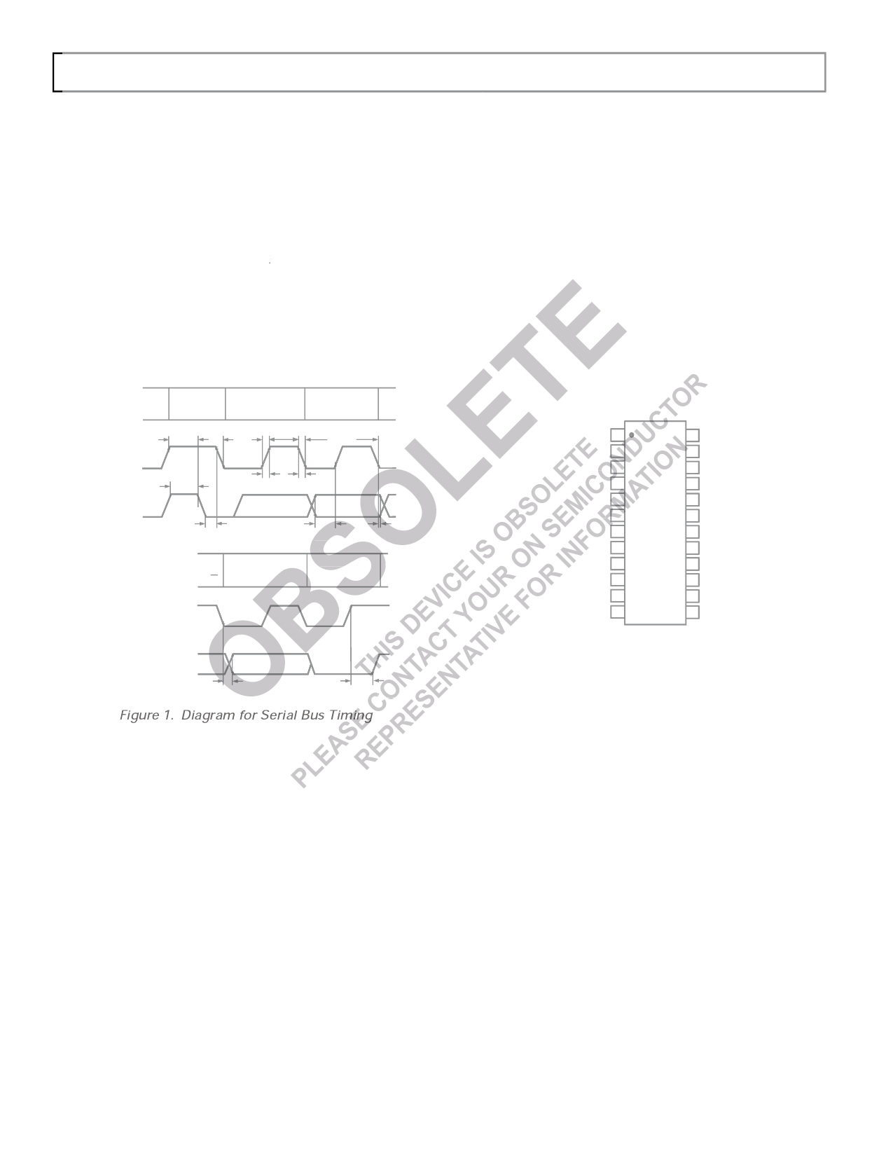
PROTOCOL
SCL
SDA
PROTOCOL
Start
Condition
(S)
tSU;STA
Bit 7
MSB
(A7)
tLOW
tHIGH
Bit 6
(A6)
1/fSCL
tBUF
tr
tf
tHD;STA
tSU;DAT
tHD;DAT
Bit 0
LSB
(R/W)
Acknowledge
(A)
Stop
Condition
(P)
SCL
PIN CONFIGURATION
NTEST_OUT/A0 1
24 VID0
A1 2
23 VID1
SDA 3
22 VID2
SCL 4
21 VID3
FAN1
FAN2
CI
5 ADM9240 20 VID4
6 TOP VIEW 19 +VCCP1
7 (Not to Scale) 18 +2.5VIN
GNDD 8
17 +3.3VIN
VCC 9
16 +5VIN
INT 10
15 +12VIN
NTEST_IN/AOUT 11
14 +VCCP2
RESET 12
13 GNDA
SDA
tVD;DAT
tSU;STO
Figure 1. Diagram for Serial Bus Timing
Maximum Junction Temperature (
Rev. 2 | Page 4 of 22 | www.onsemi.com
–4–
REV. 0
Share Link: 