ADM9240 View Datasheet(PDF) - ON Semiconductor
Part Name
Description
Manufacturer
ADM9240 Datasheet PDF : 22 Pages
| |||
ADM9240
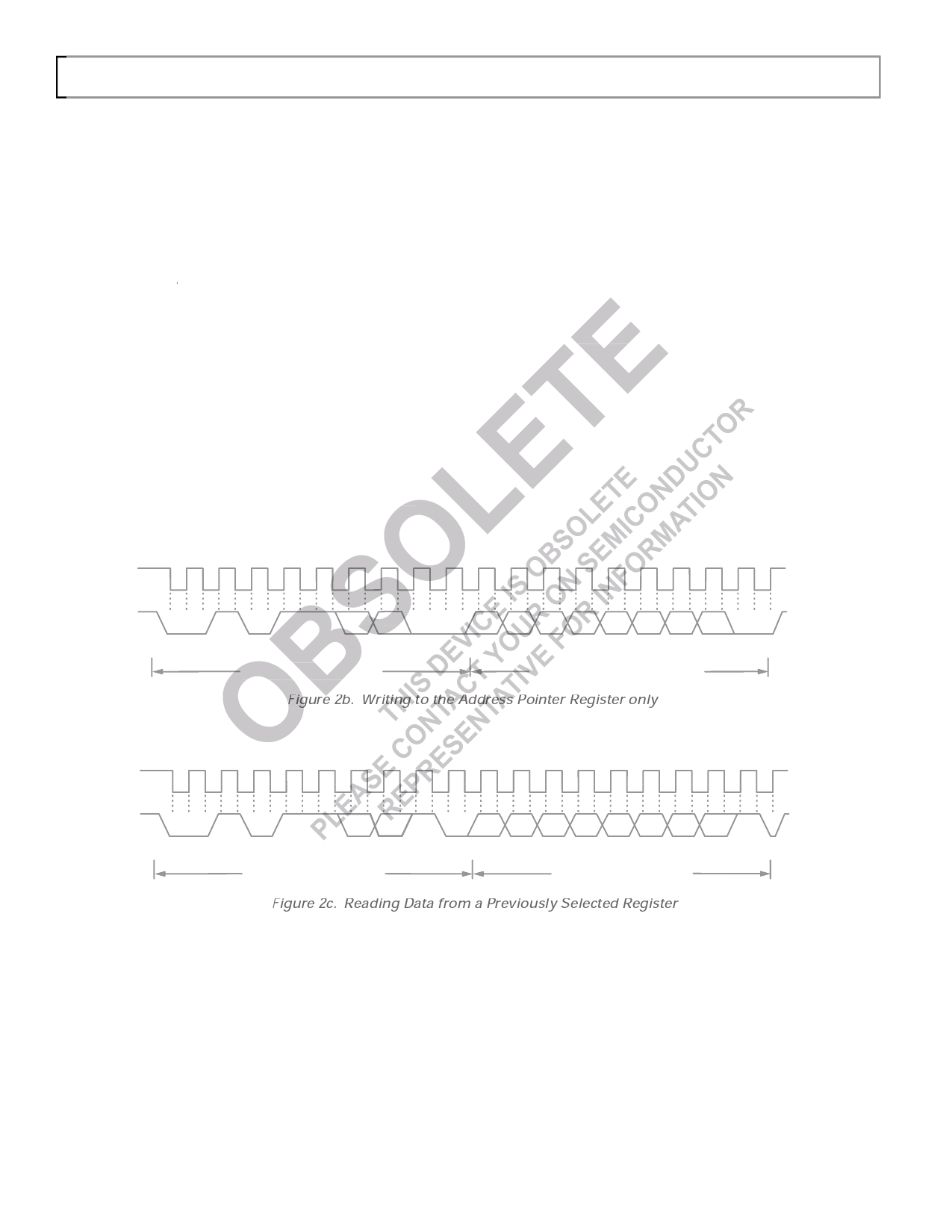
When reading data from a register there are two possibilities:
1. If the ADM9240’s Address Pointer Register value is un-
known or not the desired value, it is first necessary to set it to
the correct value before data can be read from the desired
data register. This is done by performing a write to the
ADM9240 as before, but only the data byte containing the
register address is sent, as data is not to be written to the
register. This is shown in Figure 2b.
A read operation is then performed consisting of the serial
bus address, R/W bit set to 1, followed by the data byte read
from the data register. This is shown in Figure 2c.
2. If the Address Pointer Register is known to be already at the
desired address, data can be read from the corresponding
data register without first writing to the Address Pointer
Register, so Figure 2b can be omitted.
Notes:
1. Although it is possible to read a data byte from a data register
without first writing to the Address Pointer Register, if the
Address Pointer Register is already at the correct value, it is
not possible to write data to a register without writing to the
Address Pointer Register, because the first data byte of a
write is always written to the Address Pointer Register.
2. In Figures 2a to 2c, the serial bus address is shown as the
default value 01011(A1)(A0), where A1 and A0 are
hardwired to either Logic 0 or Logic 1.
ANALOG INPUTS
The ADM9240 has six analog inputs. Four of these are dedi-
cated to monitoring the following power supply voltages: +12 V,
+5 V, +3.3 V, +2.5 V.
These inputs are multiplexed into the on-chip, successive ap-
proximation, analog-to-digital converter. This has a resolution
of ten bits, but only eight bits are used for the voltage measure-
ment and limit comparison. The basic input range of the ADC
is 0 V to 2.5 V, and the power supply inputs are scaled by on-
chip attenuators such that the ADC produces an output of 3/4 ×
full scale or 192 decimal, when the input voltage is at its nomi-
nal value. The use of on-chip scaling guarantees accuracy and
removes the need for precision external resistors.
1
9
1
9
SCL
SDA
0
START BY
MASTER
1
0
1
1 A1 A0 R/ W
D7 D6 D5 D4 D3 D2 D1 D0
ACK. BY
ADM9240
FRAME 1
SERIAL BUS ADDRESS BYTE
FRAME 2
ADDRESS POINTER REGISTER BYTE
Figure 2b. Writing to the Address Pointer Register only
ACK. BY STOP BY
ADM9240 MASTER
1
9
1
9
SCL
SDA
0
START BY
MASTER
bus address, R
1
0
1
1 A1 A0 R/ W
D7 D6 D5 D4 D3 D2 D1
FRAME 1
SERIAL BUS ADDRESS BYTE
ACK. BY
ADM9240
FRAME 2
DATA BYTE FROM ADM9240
Figure 2c. Reading Data from a Previously Selected Register
D0
NO ACK. STOP BY
BY MASTER MASTER
Rev. 2 | Page 8 of 22 | www.onsemi.com
–8–
REV. 0
Share Link: 