MB91107 View Datasheet(PDF) - Fujitsu
Part Name
Description
Manufacturer
MB91107 Datasheet PDF : 96 Pages
| |||
MB91107/108
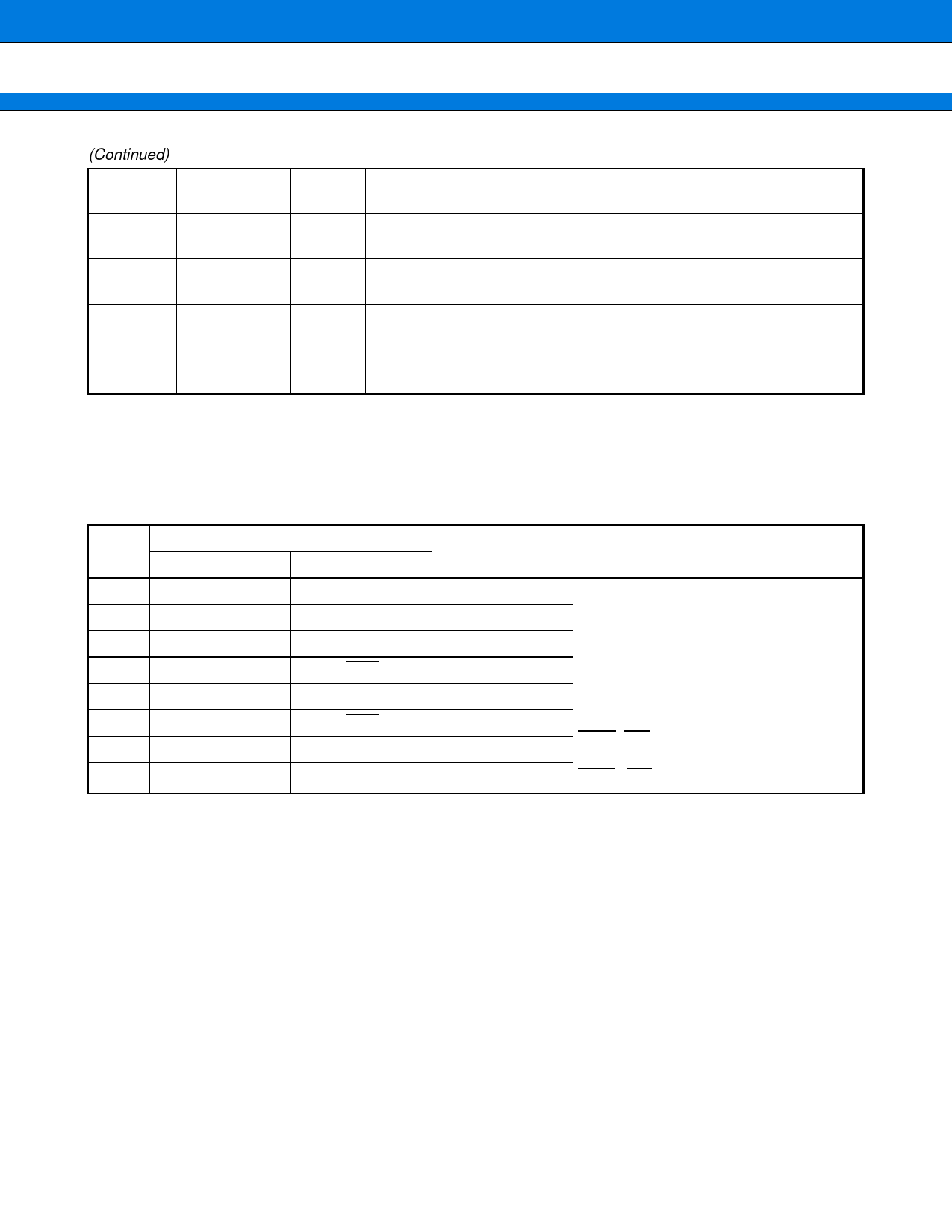
(Continued)
Pin no.
Pin name
Circuit
type
Function
11
AVSS/ AVRL
Power supply pin (VSS) for A/D converter and reference voltage input pin
(low).
24, 55,
110
VCC
Power supply pin (VCC) for digital circuit.
Always three pins must be connected to the power supply
64
C
Bypass capacitor pin for internal capacitor.
Refer to the HANDLING DEVICES.
34, 52, 75,
101, 119
VSS
Earth level (VSS) for digital circuit.
Note : In most of the above pins, I/O port and resource I/O are multiplexed e.g. xxx/Pxxx. In case of conflict between
output of I/O port and resource I/O, priority is always given to the output of resource I/O.
s DRAM CONTROL REGISTER
Pin
Data bus 16-bit mode
name 2CAS/1WR mode 1CAS/2WR mode
Data bus 8-bit
mode
RAS0 Area 4 RAS
Area 4 RAS
Area 4 RAS
RAS1 Area 5 RAS
Area 5 RAS
Area 5 RAS
CS0L Area 4 CASL
Area 4 CAS
Area 4 CAS
CS0H Area 4 CASH
Area 4 WEL
Area 4 CAS
CS1L Area 5 CASL
Area 5 CAS
Area 5 CAS
CS1H Area 5 CASH
Area 5 WEL
Area 5 CAS
DW0 Area 4 WE
Area 4 WEL
Area 4 WE
DW1 Area 5 WE
Area 5 WEL
Area 5 WE
Remarks
Correspondence of “L” “H” to lower ad-
dress 1 bit (A0) in data bus 16-bit mode.
“L”: “0”
“H”: “1”
CASL : CAS which A0 corresponds to “0”
area
CASH : CAS which A0 corresponds to “1”
area
WEL : WE which A0 corresponds to “0”
area
WEH : WE which A0 corresponds to “1”
10
Share Link: 