MB91107 View Datasheet(PDF) - Fujitsu
Part Name
Description
Manufacturer
MB91107 Datasheet PDF : 96 Pages
| |||
MB91107/108
Pin no.
80
81
82
83
84
65
66
67
68
69
70
71
56
57
58
59
60
61
62
63
76
77
78
53
54
74
73
6
Pin name
BGRNT/P81
BRQ/P82
RD
WR0
WR1/P85
CS0
CS1/PA1
CS2/PA2
CS3/PA3
CS4/PA4
CS5/PA5
CLK/PA6
RAS0/PB0
CS0L/PB1
CS0H/PB2
DW0/PB3
RAS1/PB4
CS1L/PB5
CS1H/PB6
DW1/PB7
MD0
MD1
MD2
X1
X0
RST
HST
Circuit
type
Function
External bus release acknowledge output.
F Outputs “L” level when external bus is released.
Can be configured as a port when this pin is not used.
External bus release request input.
P Inputs “1” when release of external bus is required.
Can be configured as a port when this pin is not used.
M Read strobe output pin for external bus.
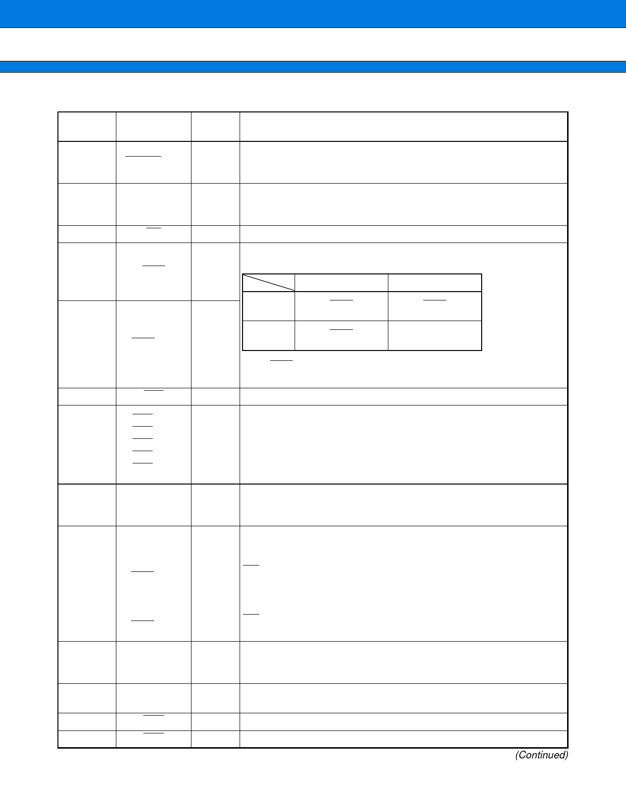
Write strobe output pin for external bus. Relation between control signals
and effective byte locations is as follows:
M
16-bit bus width 8-bit bus width
D31 to
D24
WR0
WR0
D23 to
F
D16
WR1
(I/O port enabled)
Note: WR1 is Hi-Z during resetting. Attach an external pull-up resister
when using at 16-bit bus width.
M Chip select 0 output (“L” active).
Chip select 1 output (“L” active).
Chip select 2 output (“L” active).
F
Chip select 3 output (“L” active).
Chip select 4 output (“L” active).
Chip select 5 output (“L” active).
Can be configured as ports when PA1 to PA5 are not used.
System clock output.
F Outputs clock signal of external bus operating frequency.
Can be configured as a port when PA6 is not used.
F
RAS output for DRAM bank 0.
CASL output for DRAM bank 0.
CASH output for DRAM bank 0.
WE output for DRAM bank 0 (“L” active).
RAS output for DRAM bank 1.
CASL output for DRAM bank 1.
Refer to the
DRAM interface
for details.
CASH output for DRAM bank 1.
WE output for DRAM bank 1 (“L” active)
Can be configured as a port when PB0 to PB7 are not used.
Mode pins 0 to 2.
G MCU basic operation mode is set by these pins.
Directly connect these pins with VCC or VSS for use.
A
Clock (oscillator) output.
Clock (oscillator) input.
B External reset input.
H Hardware standby input (“L” active).
(Continued)
Share Link: 