MB91107 View Datasheet(PDF) - Fujitsu
Part Name
Description
Manufacturer
MB91107 Datasheet PDF : 96 Pages
| |||
MB91107/108
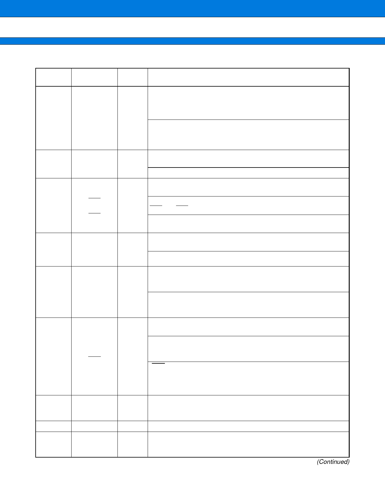
Pin no.
25
26
27
28
29
30
31
32
16
17
18
19
20
21
22
23
50
51
12 to 15
9
10
Pin name
INT0/PG0
INT1/PG1
INT2/PG2
INT3/PG3
INT4/PG4
INT5/PG5
INT6/PG6
INT7/PG7
TRG0/PH0
TRG1/PH1
TRG2/PH2/
CS6
TRG3/PH3/
CS7
OCPA0/PH4
OCPA1/PH5
OCPA2/PH6
OCPA3/PH7
DACK2/PI0
EOP2/PI1/
ATG
AN0 to AN3
AVCC
AVRH
Circuit
type
Function
(INT0 to INT7) External interrupt request input pin.
This pin is used for input during corresponding interrupt is enabled, and
it is necessary to disable output for other functions from this pin unless
I
such output is made intentionally.
(PG0 and PG7) General purpose I/O port.
(TRG0 and TRG1) PWM timer external trigger input pin.
F This function is available when PH0 and PH1 data outputs are disabled.
(PH0 and PH1) General purpose I/O port.
(TRG2 and TRG3) PWM timer external trigger input pin.
This function is available when PH2 and PH3 data outputs are disabled.
F
(PH2 and PH3) Can be configured as a I/O port when TRG2, TRG3,
CS6 and CS7 are not used.
Chip select 6 output (“L” active).
Chip select 7 output (“L” active).
(OCPA0 to OCPA3) PWM timer output pin.
F
This function is available when PWM timer output is enabled.
(PH4 to PH7) General purpose I/O port.
(DACK2) External transfer request acknowledge output pin for DMAC
(ch. 2). This function is available when transfer request output for DMAC
is enabled.
F
(PI0) General purpose I/O port.
This function is available when transfer request acknowledge output for
DMAC or DACK2 output is disabled.
(EOP2) EOP output pin for DMAC (ch.1).
This function is available when EOP output for DMAC is enabled.
(PI1) General purpose I/O port.
This function is available when transfer complete acknowledge output
F for DMAC output is disabled.
(ATG)External trigger input pin for A/D converter.
This pin is used for input when external trigger is selected to cause A/D
converter operation, and it is necessary to disable output for other func-
tions from this pin unless such output is made intentionally.
(AN0 to AN3) Analog input pins of A/D converter.
N This function is available when AIC register is set to specify analog input
mode.
Power supply pin (VCC) for A/D converter.
Reference voltage input (high) for A/D converter.
Make sure to turn on and off this pin with potential of AVRH or more ap-
plied to VCC.
(Continued)
9
Share Link: 