DSP1620 View Datasheet(PDF) - Agere -> LSI Corporation
Part Name
Description
Manufacturer
DSP1620 Datasheet PDF : 114 Pages
| |||
DSP1628 Digital Signal Processor
Preliminary Data Sheet
February 1997
3 Pin Information (continued)
Functional descriptions of pins 1—100 are found in Section 6, Signal Descriptions. The functionality of CKI and CKI2
pins are mask-programmable (see Section 7, Mask-Programmable Options). Input levels on all I and I/O type pins
are designed to remain at full CMOS levels when not driven by the DSP.
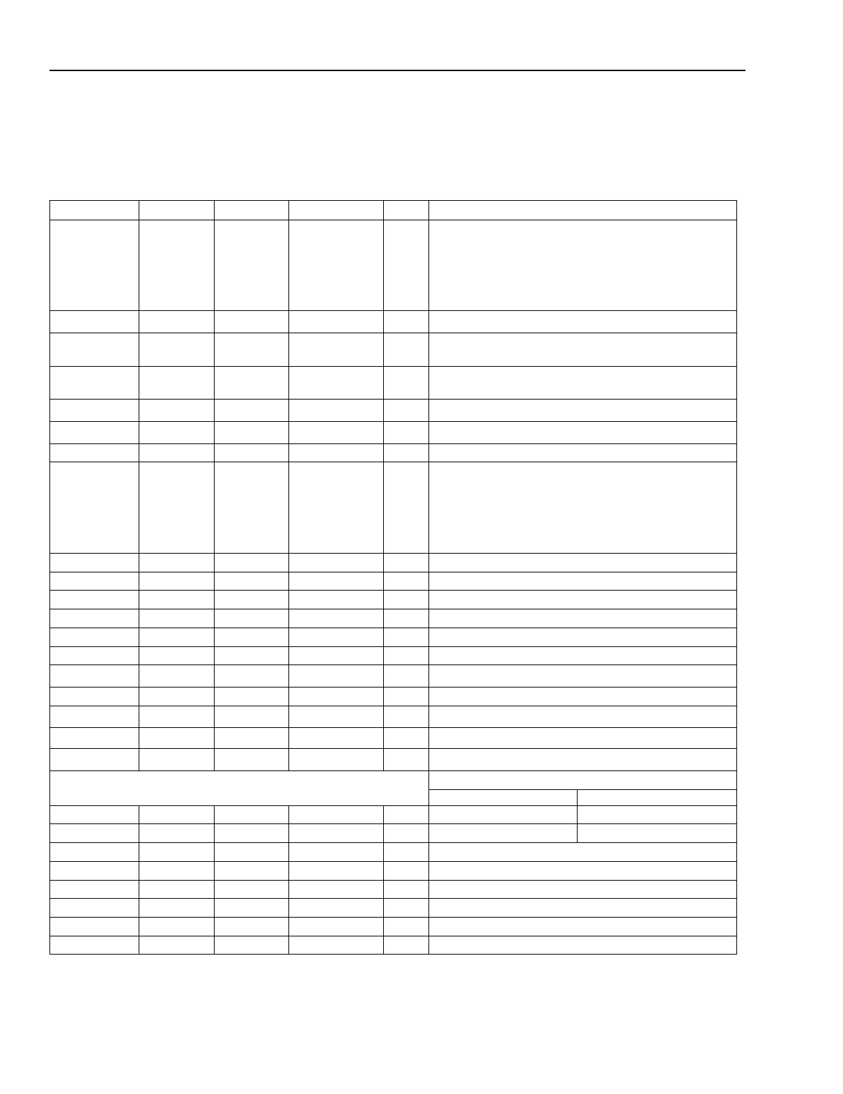
Table 1. Pin Descriptions
PBGA Pin BQFP Pin TQFP Pin Symbol Type
Name/Function
B6, A6, B5,
A5, B4, A4,
B3, A3, B2,
A2, A1, B1,
C2, C1, C3,
D1
D2
E1
1, 2, 3, 4,
5, 7, 8, 9,
10, 11, 12,
15, 16, 17,
18, 19
20
21
88, 89, 90,
91, 92, 94,
95, 96, 97,
98, 99, 2,
3, 4, 5, 6
7
8
E2
23
10
F1
F2
G1
G2, H1, H2,
J1, J2, K1,
K2, L1, L2,
M1, K3, M2,
L3, M3, L4,
M4
L5
M5
L6
M6
L7
M7
L8
M8
24
25
27
28, 29, 31,
32, 33, 34,
35, 36, 37,
40, 41, 42,
43, 44, 45,
46
47
48
50
51
52
53
54
56
11
12
14
15, 16, 18,
19, 20, 21,
22, 23, 24,
27, 28, 29,
30, 31, 32,
33
34
35
37
38
39
40
41
43
DB[15:0]
IO
ERAMHI
ERAMLO
EROM
RWN
EXM
AB[15:0]
INT1
INT0
IACK
STOP
TRAP
RSTB
CKO
TCK
I/O* External Memory Data Bus 15—0.
O† Data Address 0x4000 to 0x40FF I/O Enable.
O† Data Address 0x8000 to 0xFFFF External RAM
Enable.
O† Data Address 0x4100 to 0x7FFF External RAM
Enable.
O† Program Address External ROM Enable.
O† Read/Write Not.
I External ROM Enable.
O* External Memory Address Bus 15—0.
I Vectored Interrupt 1.
I Vectored Interrupt 0.
O* Interrupt Acknowledge.
I STOP Input Clock.
I/O* Nonmaskable Program Trap/Breakpoint Indication.
I Reset Bar.
O† Processor Clock Output.
I JTAG Test Clock.
L9
57
44
TMS
I‡ JTAG Test Mode Select.
M9
58
45
TDO
O§ JTAG Test Data Output.
L10
59
46
TDI
I‡ JTAG Test Data Input.
Mask-Programmable Input Clock Option
CMOS
Small Signal
L11
61
48
CKI**
I
CKI
VAC
M11
62
49
CKI2**
I
VSSA
VCM
K10
65
52
VEC0/IOBIT7 I/O* Vectored Interrupt Indication 0/Status/Control Bit 7.
L12
66
53
VEC1/IOBIT6 I/O* Vectored Interrupt Indication 1/Status/Control Bit 6.
K11
67
54
VEC2/IOBIT5 I/O* Vectored Interrupt Indication 2/Status/Control Bit 5.
K12
68
55
VEC3/IOBIT4 I/O* Vectored Interrupt Indication 3/Status/Control Bit 4.
J11
69
56
IOBIT3/PB7 I/O* Status/Control Bit 3/PHIF Data Bus Bit 7.
J12
70
57
IOBIT2/PB6 I/O* Status/Control Bit 2/PHIF Data Bus Bit 6.
* 3-states when RSTB = 0, or by JTAG control.
† 3-states when RSTB = 0 and INT0 = 1. Output = 1 when RSTB = 0 and INT0 = 0, except CKO which is free-running.
‡ Pull-up devices on input.
§ 3-states by JTAG control.
** See Section 7, Mask-Programmable Options.
†† For SIO multiprocessor applications, add 5 kΩ external pull-up resistors to SADD1 and/or SADD2 for proper initialization.
6
Lucent Technologies Inc.
Share Link: 