DSP1620 View Datasheet(PDF) - Agere -> LSI Corporation
Part Name
Description
Manufacturer
DSP1620 Datasheet PDF : 114 Pages
| |||
Preliminary Data Sheet
February 1997
DSP1628 Digital Signal Processor
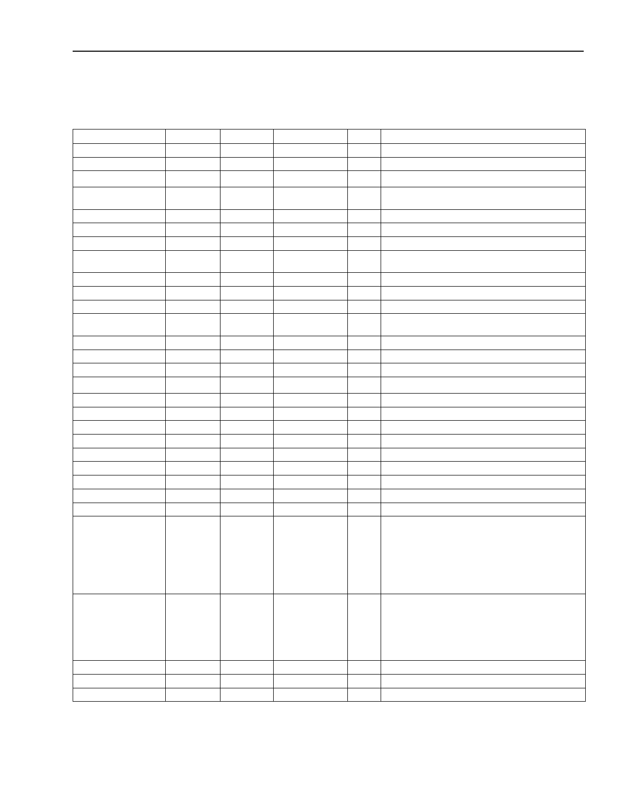
3 Pin Information (continued)
Functional descriptions of pins 1—100 are found in Section 6, Signal Descriptions.
Table 1. Pin Descriptions (continued)
PBGA Pin
BQFP Pin TQFP Pin Symbol Type
Name/Function
H11
71
58
IOBIT1/PB5 I/O* Status/Control Bit 1/PHIF Data Bus Bit 5.
H12
72
59
IOBIT0/PB4 I/O* Status/Control Bit 0/PHIF Data Bus Bit 4.
G11
73
60
TRST
I‡ JTAG Test Reset.
G12
74
61
SADD2/PB3†† I/O* SIO2 Multiprocessor Address/PHIF Data Bus
Bit 3.
F11
75
62
DOEN2/PB2 I/O* SIO2 Data Output Enable/PHIF Data Bus Bit 2.
F12
77
64
DI2/PB1
I/O* SIO2 Data Input/PHIF Data Bus Bit 1.
E11
78
65
ICK2/PB0 I/O* SIO2 Input Clock/PHIF Data Bus Bit 0.
E12
79
66
OBE2/POBE O* SIO2 Output Buffer Empty/PHIF Output Buffer
Empty.
D11
80
67
IBF2/PIBF
O* SIO2 Input Buffer Full/PHIF Input Buffer Full.
D12
81
68
OLD2/PODS I/O* SIO2 Output Load/PHIF Output Data Strobe.
C11
82
69
ILD2/PIDS I/O* SIO2 Input Load/PHIF Input Data Strobe.
C12
83
70
SYNC2/PBSEL I/O* SIO2 Multiprocessor Synchronization/PHIF
Byte Select.
C10
84
71
DO2/PSTAT I/O* SIO2 Data Output/PHIF Status Register Select.
B12
85
72
OCK2/PCSN I/O* SIO2 Output Clock/PHIF Chip Select Not.
B11
86
73
DOEN1
I/O* SIO1 Data Output Enable.
A12
87
74
SADD1††
I/O* SIO1 Multiprocessor Address.
A11
90
77
SYNC1
I/O* SIO1 Multiprocessor Synchronization.
B10
91
78
DO1
O* SIO1 Data Output.
A10
92
79
OLD1
I/O* SIO1 Output Load.
B9
93
80
OCK1
I/O* SIO1 Output Clock.
A9
94
81
ICK1
I/O* SIO1 Input Clock.
B8
95
82
ILD1
I/O* SIO1 Input Load.
A8
96
83
DI1
I SIO1 Data Input.
B7
98
85
IBF1
O* SIO1 Input Buffer Full.
A7
D4, D5, D6, D7, D8,
E4, E5, E6, E7, E8,
E9, F4, F5, F6, F7,
F8, F9, G4, G5, G6,
G7, G8, G9, H4,
H5, H6, H7, H8, H9,
J4, J5, J6, J7, J8, J9
C4, C5, C6, C7, C8,
D3, D9, D10, E3,
E10, F3, F10, G3,
G10, H3, H10, J3,
J10, K4, K5, K6, K7,
K8, K9,
99
6, 14, 26,
38, 49, 64,
76, 89, 97
13, 22, 30,
39, 55, 88,
100
86
93, 1, 13,
25, 36, 51,
63, 76, 84
100, 9, 17,
26, 42, 75,
87
OBE1
VSS
VDD
O* SIO1 Output Buffer Empty.
P Ground.
P Power Supply.
M10
60
47
VDDA
P Analog Power Supply.
M12
63
50
VSSA
P Analog Ground.
C9
—
—
—
— No Die Connect—unused.
* 3-states when RSTB = 0, or by JTAG control.
† 3-states when RSTB = 0 and INT0 = 1. Output = 1 when RSTB = 0 and INT0 = 0, except CKO which is free-running.
‡ Pull-up devices on input.
§ 3-states by JTAG control.
** See Section 7, Mask-Programmable Options.
†† For SIO multiprocessor applications, add 5 kΩ external pull-up resistors to SADD1 and/or SADD2 for proper initialization.
Lucent Technologies Inc.
7
Share Link: 