CXD2434ATQ View Datasheet(PDF) - Sony Semiconductor
Part Name
Description
Manufacturer
CXD2434ATQ Datasheet PDF : 26 Pages
| |||
CXD2434ATQ
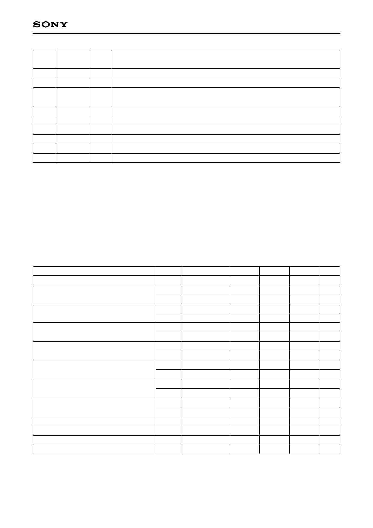
Pin No. Symbol
40
CKO
41 RESET
42 STDBY
43
TRIG
44
ESG
45
EFS
46
HD
47
VD
48 TEST2
I/O
Description
O 1560 fH clock output.
I RESET. (With pull-up resistor) Low : Reset, High : Normal
Standby. (With pull-up resistor)
I
Low: Internal clock supply stopped, High: Normal
I External trigger input. (With pull-up resistor)
I External readout input. (With pull-up resistor)
I Vertical CCD discharge input. (With pull-up resistor)
I Horizontal sync signal input.
I Vertical sync signal input.
I Test. (With pull-up resistor)
Electrical Characteristics
1. DC Characteristics
VDD=4.75 V to 5.25 V Topr= –20 to +75 °C
Item
Symbol Conditions
Supply voltage
VDD
Input voltage 1
VIH1
(Input pins other than those listed below) VIL1
Input voltage 2
VIH2
(Pin 2)
VIL2
Output voltage 1
VOH1 IOH=–2.5 mA
(Output pins other than those listed below) VOL1 IOL=4.5 mA
Output voltage 2
VOH2 IOH=–5.0 mA
(Pins 21, 22, 23, 38, 39 and 40)
VOL2 IOL=9.0 mA
Output voltage 3
VOH3 IOH=–7.5 mA
(Pin 10)
VOL3 IOL=13.5 mA
Output voltage 4
VOH4 IOH=–14.0 mA
(Pins 13 and 14)
VOL4 IOL=24.0 mA
Output voltage 5
VOH5
(Pin 1)
VOL5
Feedback resistor
RFB VIN=VSS or VDD
Pull-up resistor
RPU VIL=0 V
Pull-down resistor
RPD VIH=VDD
Current consumption
IDD VDD=5 V
Min.
4.75
0.7 VDD
0.7 VDD
VDD–0.4
VDD–0.4
VDD–0.4
VDD–0.4
VDD/2
Typ.
5.0
1M
50 k
50 k
40
Max. Unit
5.25
V
V
0.3 VDD V
V
0.3 VDD V
V
0.4
V
V
0.4
V
V
0.4
V
V
0.4
V
V
VDD/2
V
Ω
100 k Ω
100 k Ω
mA
—4—
Share Link: 