UPSD3212A(2009) View Datasheet(PDF) - STMicroelectronics
Part Name
Description
Manufacturer
UPSD3212A
(Rev.:2009)
(Rev.:2009)
STMicroelectronics

UPSD3212A Datasheet PDF : 181 Pages
| |||
UPSD3212A, UPSD3212C, UPSD3212CV
UPSD321xx description
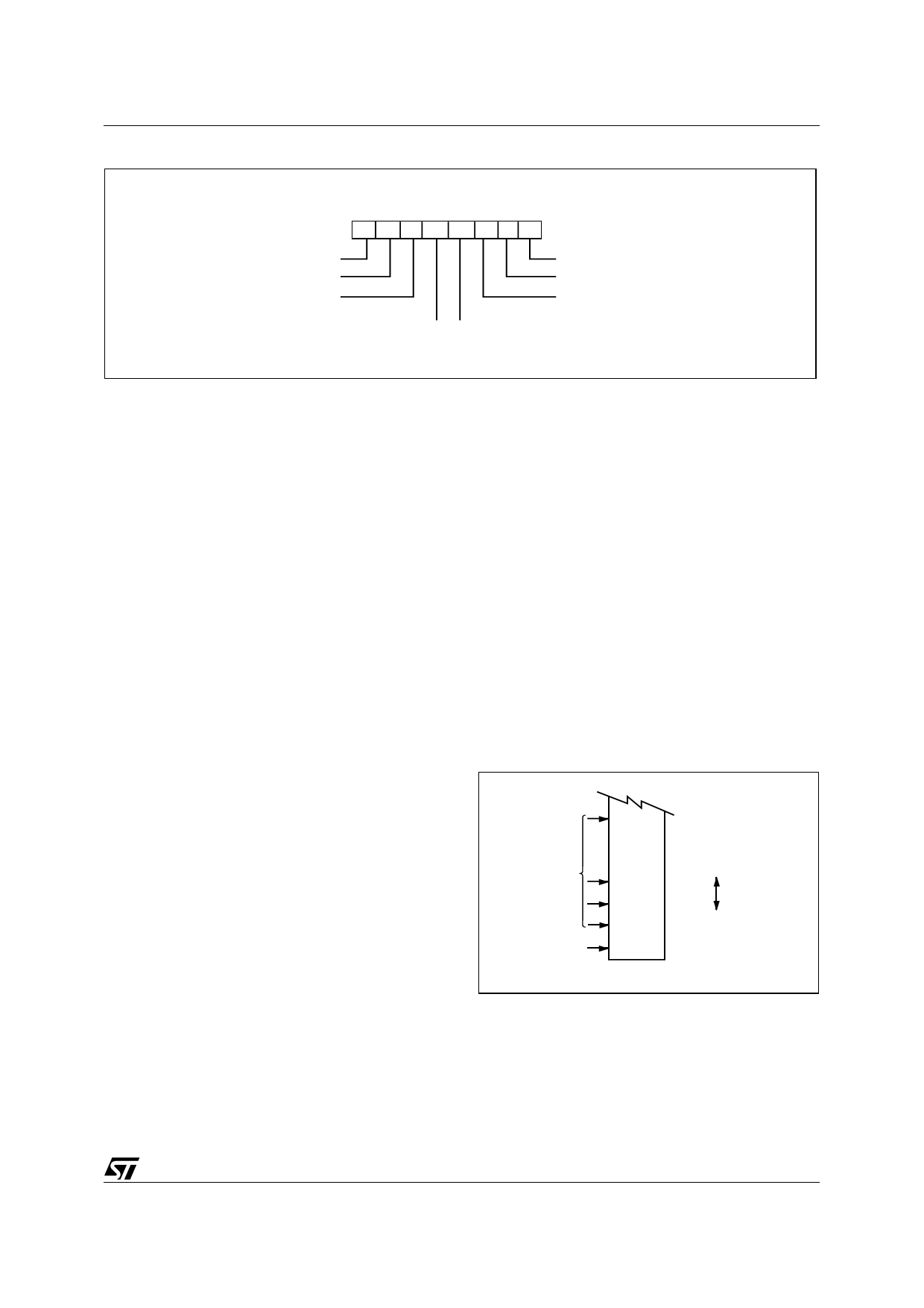
Table 2. 80-pin package pin description (continued)
Port Signal Pin In/
pin name no. out
Basic
Function
Alternate
JTAG
TMS
20
I JTAG pin
JTAG
TCK
16
I JTAG pin
PC3 TSTAT 14 I/O General I/O port pin
PC4 TERR_ 9 I/O General I/O port pin
JTAG
TDI
7
I JTAG pin
PLD macrocell outputs
PLD inputs
JTAG pins are dedicated
pins
JTAG
TDO
6
O JTAG pin
PC7
5 I/O General I/O port pin
PD1 CLKIN 3 I/O General I/O port pin
PLD I/O
Clock input to PLD and
APD
PD2
1 I/O General I/O port pin
PLD I/O
Chip select to PSD module
Vcc
12
Vcc
50
GND
13
GND
29
GND
69
USB+ 10
NC
11
NC
17
NC
71
1.1
52-pin package I/O port
The 52-pin package members of the UPSD321xx devices have the same port pins as those
of the 80-pin package except:
● Port 0 (P0.0-P0.7, external address/data bus AD0-AD7)
● Port 2 (P2.0-P2.3, external address bus A8-A11)
● Port A (PA0-PA7)
● Port D (PD2)
● Bus control signal (RD,WR,PSEN,ALE)
● Pin 5 requires a pull-up resistor (2 kΩ for 3 V devices, 7.5 kΩ for 5 V devices) for all
devices, with or without USB function.
15/181
Share Link: