KAD2710L-17 View Datasheet(PDF) - Unspecified
Part Name
Description
Manufacturer
KAD2710L-17 Datasheet PDF : 17 Pages
| |||
KAD2710L 10-Bit, 275MSPS Analog-to-Digital Converter
The value of the shunt resistor should be determined
based on the desired termination impedance. The
differential input impedance of the KAD2710 is 10MΩ.
A differential amplifier can be used in applications
that require dc coupling, at the expense of reduced
dynamic performance. In this configuration the am-
plifier will typically reduce the achievable SNR and
distortion performance. A typical differential amplifier
configuration is shown in Figure 20.
rate, then use the KAD2710L's divide-by-2 to generate
a 50%-duty-cycle clock. The divider only uses the ris-
ing edge of the clock, so 50% clock duty cycle is as-
sured .
CLKDIV Pin
AVSS
AVDD
Divide Ratio
2
1
Table 3. CLKDIV Pin Settings
Jitter
In a sampled data system, clock jitter directly im-
pacts the achievable SNR performance. The theoreti-
cal relationship between clock jitter and maximum
SNR is shown in Equation 1 and is illustrated in Figure
22.
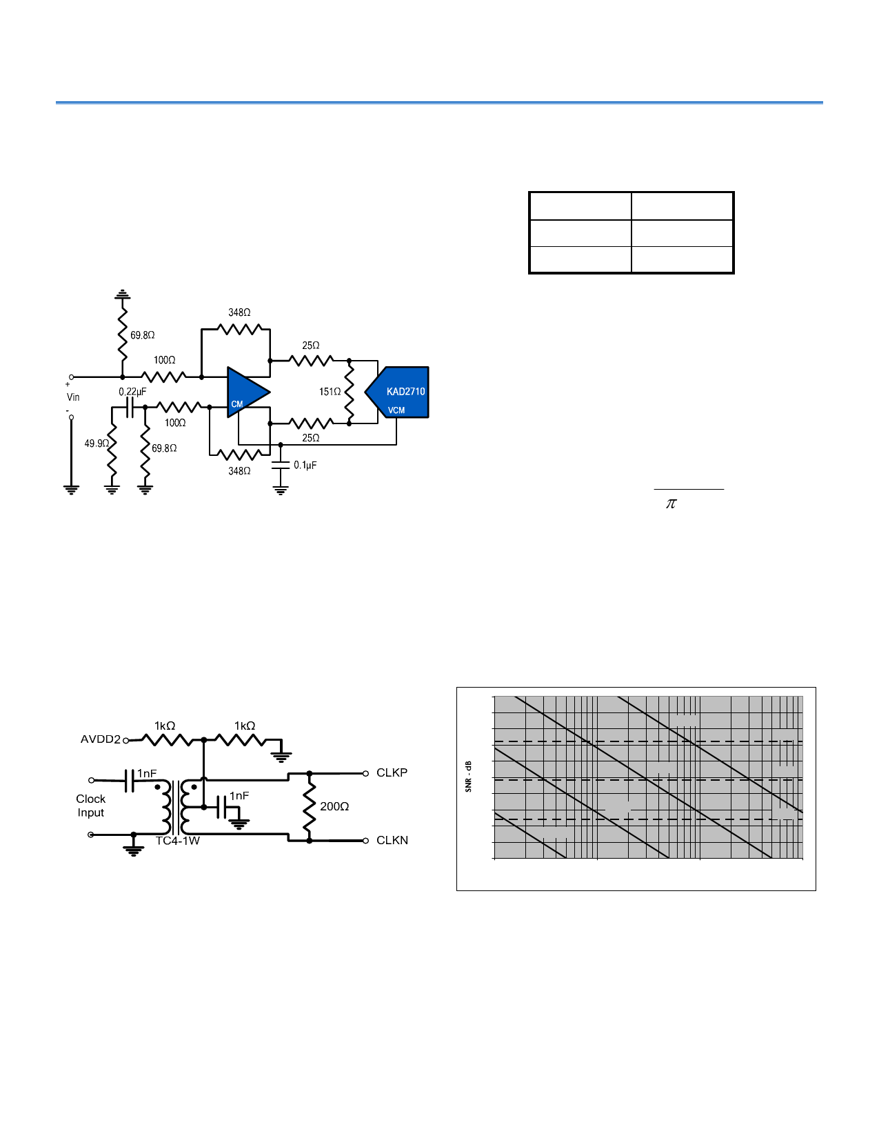
Figure 20. Differential Amplifier Input
Clock Input
The clock input circuit is a differential pair (see Figure
24). Driving these inputs with a high level (up to 1.8VPP
on each input) sine or square wave will provide the
lowest jitter performance. The recommended drive
circuit is shown in Figure 21. The clock inputs can be
driven single-ended, but this is not recommended as
performance will suffer.
Figure 21. Recommended Clock drive
The CLKDIV pin is a 1.8V CMOS control pin (input)
that selects whether the input clock frequency is
passed directly to the ADC or divided by two. Apply-
ing a low level will divide by two; 1.8V applied (or left
floating) will not divide.
Use of the clock divider is optional. The KAD2710L's
ADC requires a clock with 50% duty cycle for opti-
mum performance. If such a clock is not available,
one option is to generate twice the desired sampling
Rev 1.1
SNR
= 20 log 10 ⎜⎜⎝⎛ 2π
1
f IN tJ
⎟⎟⎠⎞
Where tj is the RMS uncertainty in the sampling instant.
Equation 1.
This relationship shows the SNR that would be
achieved if clock jitter were the only non-ideal fac-
tor. In reality, achievable SNR is limited by internal
factors such as dc linearity (DNL), aperture jitter and
thermal noise.
100
95
90
85
80
75
70
65
60
55
50
1
tj=0.1ps
tj=1ps
tj=100ps
tj=10ps
10
100
Input Frequency - MHz
14 Bits
12 Bits
10 Bits
1000
Figure 22. SNR vs. Clock Jitter
Any internal aperture jitter combines with the input
clock jitter, in a root-sum-square fashion since they
are not statistically correlated, and this determines
the total jitter in the system. The total jitter, combined
with other noise sources, then determines the achiev-
able SNR.
Page 13 of 17
Share Link: 