KAD2710L-10 View Datasheet(PDF) - Renesas Electronics
Part Name
Description
Manufacturer
KAD2710L-10 Datasheet PDF : 17 Pages
| |||
KAD2710L
0.01µF
Analog
In
ADT1-1WT
ADT1-1WT
50O
0.1µF
KAD2710L
VCM
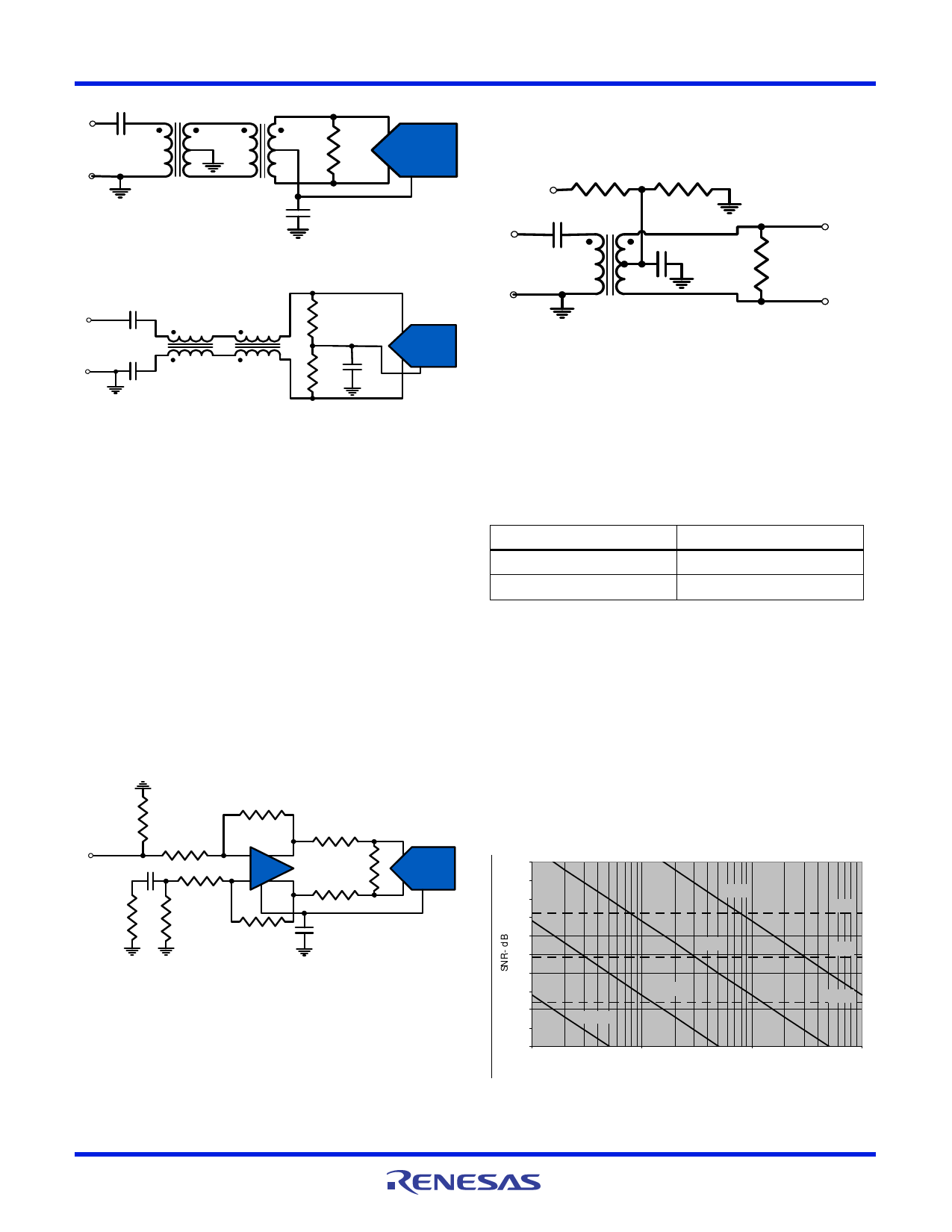
FIGURE 23. TRANSFORMER INPUT, GENERAL APPLICATION
Analog 1000pF
Input 1000pF
ADTL1-12
ADTL1-12
25O
25O
0.1µF
KAD2710L
VCM
FIGURE 24. TRANSFORMER INPUT FOR HIGH IF
APPLICATIONS
A back-to-back transformer scheme is used to improve
common-mode rejection, which keeps the common-mode level
of the input matched to VCM. The value of the shunt resistor
should be determined based on the desired load impedance.
The sample and hold circuit design uses a switched capacitor
input stage, which creates current spikes when the sampling
capacitance is reconnected to the input voltage. This creates a
disturbance at the input which must settle before the next
sampling point. Lower source impedance will result in faster
settling and improved performance. Therefore a 1:1
transformer and low shunt resistance are recommended for
optimal performance.
A differential amplifier can be used in applications that require
dc coupling. In this configuration the amplifier will typically
determine the achievable SNR and distortion. A typical
differential amplifier circuit is shown in Figure 25.
69.8O
100O
Analog
Input
0.22µF
100O
49.9O
69.8O
348O
CM
348O
25O
217O
25O
0.1µF
KAD2710
VCM
FIGURE 25. DIFFERENTIAL AMPLIFIER INPUT
Clock Input
The sample clock input circuit is a differential pair (see Figure
29). Driving these inputs with a high level (up to 1.8VPP on
each input) sine or square wave will provide the lowest jitter
performance.
The recommended drive circuit is shown in Figure 26. The
clock can be driven single-ended, but this will reduce the edge
rate and may impact SNR performance.
1kO
1kO
AVDD2
1nF
Clock
1nF
Input
TC4-1W
200O
CLKP
CLKN
FIGURE 26. RECOMMENDED CLOCK DRIVE
Use of the clock divider is optional. The KAD2710L's ADC
requires a clock with 50% duty cycle for optimum performance.
If such a clock is not available, one option is to generate twice
the desired sampling rate and use the KAD2710L's divide-by-2
setting. This frequency divider uses the rising edge of the
clock, so 50% clock duty cycle is assured. Table 2 describes
the CLKDIV connection.
TABLE 2. CLKDIV PIN SETTINGS
CLKDIV PIN
DIVIDE RATIO
AVSS
2
AVDD
1
CLKDIV is internally pulled low, so a pull-up resistor or logic
driver must be connected for undivided clock.
Jitter
In a sampled data system, clock jitter directly impacts the
achievable SNR performance. The theoretical relationship
between clock jitter (tJ) and SNR is shown in Equation 1 and is
illustrated in Figure 27.
SNR = 20 log102--------f-1-I--N----t--J-
(EQ. 1)
Where tJ is the RMS uncertainty in the sampling instant.
10 0
95
90
85
80
75
70
65
60
55
50
1
tj=0.1p s
tj=1 ps
tj=10 0p s
tj=1 0p s
10
10 0
Input Frequency - MHz
1 4 Bits
1 2 Bits
10 Bits
10 00
FIGURE 27. SNR vs CLOCK JITTER
FN6818 Rev 0.00
December 5, 2008
Page 13 of 17
Share Link: 