M2V56S20AKT-5 View Datasheet(PDF) - MITSUBISHI ELECTRIC
Part Name
Description
Manufacturer
M2V56S20AKT-5 Datasheet PDF : 51 Pages
| |||
SDRAM (Rev.1.31)
Single Data Rate
Apr. '02
MITSUBISHI LSIs
M2V56S20/ 30/ 40 ATP
M2V56S20/ 30/ 40 AKT
256M Synchronous DRAM
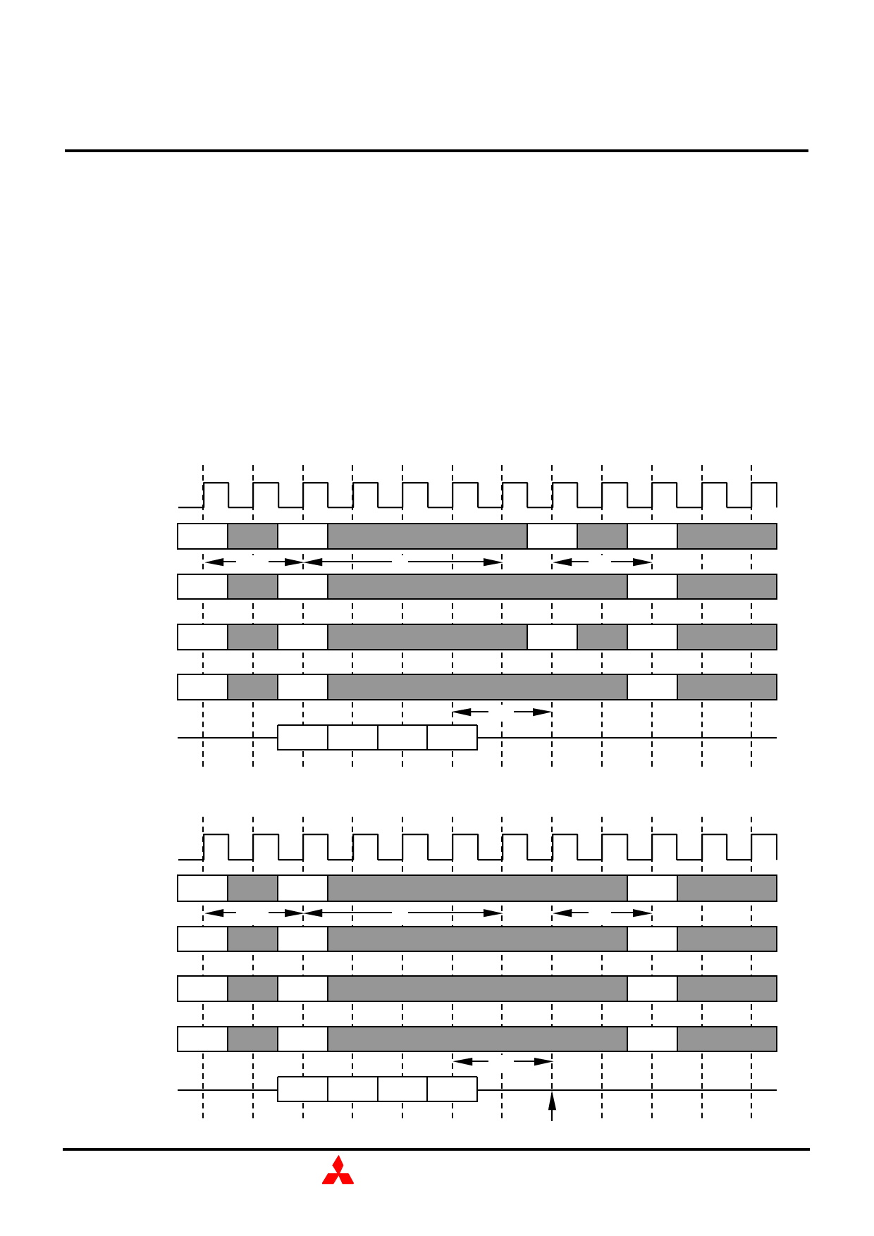
WRITE
A WRITE command can be issued to any active bank.The start address is specified by A0-9,11(x4),
A0-9 (x8), A0-8 (x16). 1st input data is set at the same cycle as the WRITE. The consecutive data length
to be written is defined by the Burst Length. The address sequence of burst data is defined by the Burst
Type. Minimum delay time of a WRITE command after an ACT command to the same bank is tRCD.
From the last input data to the PRE command, the write recovery time (tWR) is required. When A10 is
high at a WRITE command, auto-precharge (WRITEA) is performed. Any command (READ, WRITE,
PRE, ACT, TBST) to the same bank is inhibited till the internal precharge is complete. The internal
precharge starts at tWR after the last input data cycle. The next ACT command can be issued after (BL
+ tWR -1 +tRP) from the previous WRITEA. In any case, tRCD + BL + tWR -1 > tRASmin must be
met.
Write (BL=4)
CLK
Command ACT
Write
tRCD
BL
A0-9,11-12 Xa
Ya
PRE
tRP
ACT
Xa
A10 Xa
0
0
Xa
BA0-1 00
00
00
tWR
DQ
Da0 Da1 Da2 Da3
Write with Auto-Precharge (BL=4)
CLK
Command ACT
Write
tRCD
BL
A0-9,11-12 Xa
Ya
ACT
tRP
Xa
A10 Xa
1
Xa
BA0-1 00
DQ
00
00
tWR
Da0 Da1 Da2 Da3
internal precharge starts
MITSUBISHI ELECTRIC
19
Share Link: 