BT865A View Datasheet(PDF) - Unspecified
Part Name
Description
Manufacturer
BT865A Datasheet PDF : 69 Pages
| |||
CIRCUIT DESCRIPTION
Pin Descriptions
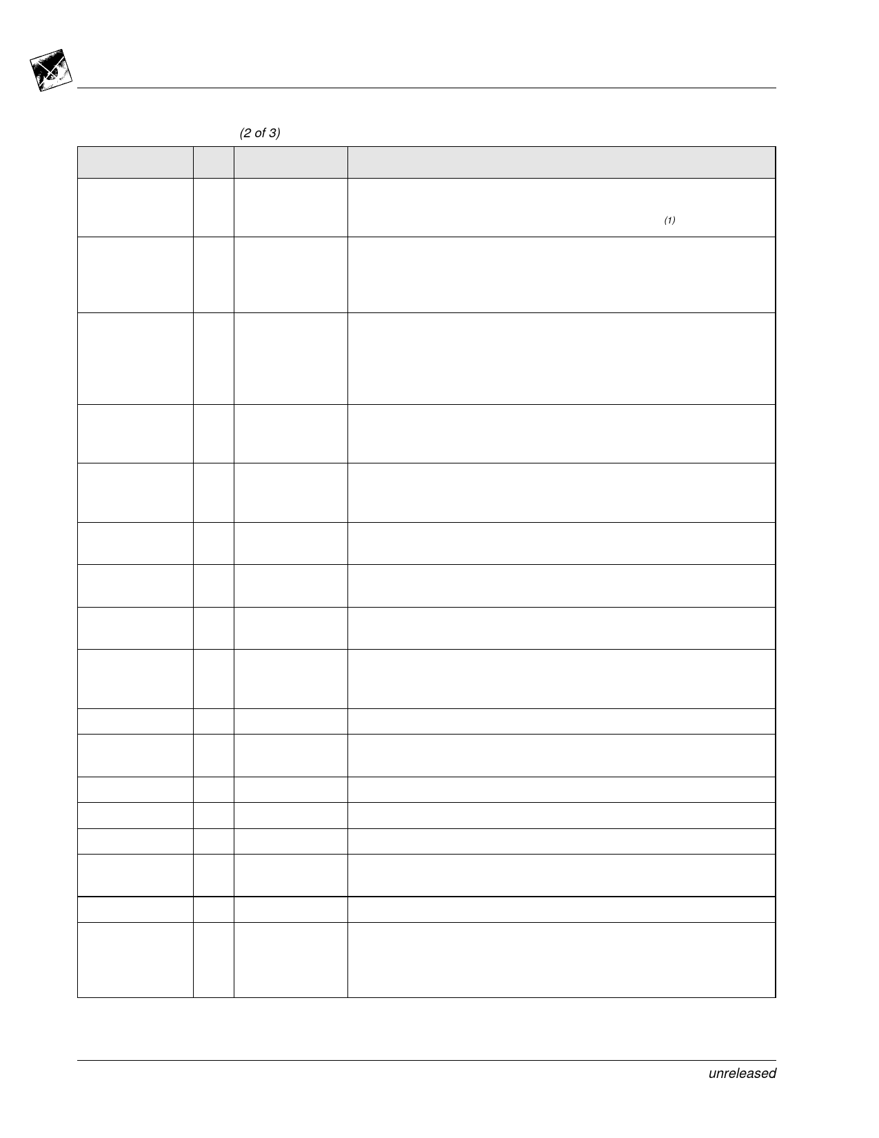
Table 1. Pin Assignments (2 of 3)
Pin Name
I/O
Pin #
ALTADDR
I 26
SLAVE
I 42
RGBOUT
I 14
FIELD
O 15
SLEEP
I 39
SDA
SCL
VDD3V
CVBS/B
I/O 40
I 41
I 44
O8
AGND (CVBS/B)
CVBS/G
6
O 10
AGND (CVBS/G)
7
C/R
O 12
AGND (C/R)
9
Y/CVBS
O 13
AGND (Y/CVBS)
11
FSADJUST
I1
Bt864A/865A
YCrCb to NTSC/PAL Digital Video Encoder
Description
Alternate slave address input (TTL compatible). A logical one configures
the device to respond to an I2C address of 0x88; a logical zero config-
ures the device to respond to an I2C address of 0x8A.(1)
Slave/master mode select input (TTL compatible). A logical one config-
ures the device for slave video timing operation. A logical zero config-
ures the device for master video timing operation. This pin may be
connected directly to VDD or GND.
Analog RGB control input (TTL compatible). A logical one configures the
device to output analog RGB (RGBOUT mode) and one composite
video output. A logical zero configures the device to generate S-video
along with two composite video outputs. This pin may be connected
directly to VDD or GND.
Field control output (TTL compatible). FIELD transitions after the rising
edge of CLK, two clock cycles following falling HSYNC*. It is a logical
zero during FIELD 1 and is a logical one during FIELD 2.
Power-down control input (TTL compatible). A logical one configures the
device for power-down mode. A logical zero configures the device for
normal operation. This pin may be connected directly to VDD or GND.
Serial interface data input/output (TTL compatible). Data is written to
and read from the device via this serial bus.
Serial interface clock input (TTL compatible). The maximum clock rate is
100 kHz.
Input threshold adjustment. When low, indicates nominal supply voltage
of 5 volts. When high, indicates nominal supply voltage of 3.3 volts.
Composite video or Blue (with blanking and sync, and optionally, Macro-
vision encoding). Optional luma delay channel for composite video out-
put.
Analog ground for pin CVBS/B.
Composite video or Green (with blanking and sync, and optionally, Mac-
rovision encoding).
Analog ground for pin CVBS/G.
Modulated chrominance, or Red.
Analog ground for pin C/R.
Luminance or composite video (with blanking, sync, and optionally, Mac-
rovision encoding, and/or closed-captioning encoding).
Analog ground for pin Y/CVBS.
Full-scale adjust control pin. A resistor (RSET) connected between this
pin and GND controls the full-scale output current on the analog out-
puts. For standard operation, use the nominal RSET values shown
under Recommended Operating Conditions.
2
L865A_A unreleased
Share Link: 