CXD2589Q View Datasheet(PDF) - Sony Semiconductor
Part Name
Description
Manufacturer
CXD2589Q Datasheet PDF : 61 Pages
| |||
CD Digital Signal Processor
CXD2589Q
Description
The CXD2589Q is a digital signal processor LSI for
CD players and is equipped with built-in digital
filters, zero detection circuit, 1-bit DAC, and analog
low-pass filter on a single chip.
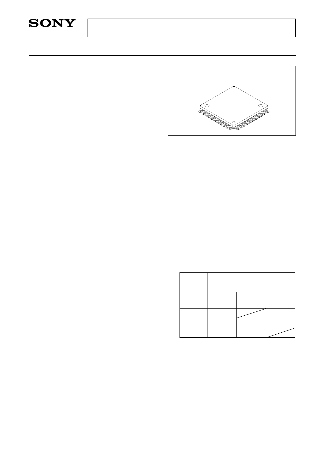
80 pin QFP (Plastic)
Features
Digital Signal Processor (DSP) Block
• Playback mode supporting CAV
(Constant Angular Velocity)
– Frame jitter-free
– Allows 0.5 to double-speed continuous playback
– Allows relative rotational velocity readout
– Supports external spindle control
• Wide capture range playback mode
– Spindle rotational velocity following method
– Supports normal-speed and double-speed playback
• 16K RAM
• EFM data demodulation
• Enhanced EFM frame sync protection
• SEC strategy-based error correction
• Subcode demodulation and Sub Q data error
detection
• Digital spindle servo
• 16-bit traverse counter
• Asymmetry compensation circuit
• Serial bus-based CPU interface
• Error correction monitor signals, etc. are output
from a new CPU interface.
• Servo auto sequencer
• Digital audio interface output
• Digital peak meter
Absolute Maximum Ratings
• Supply voltage VDD
–0.3 to +7.0
V
• Input voltage VI
–0.3 to +7.0
V
(Vss – 0.3V to VDD + 0.3V)
• Output voltage VO
–0.3 to +7.0
V
• Storage temperature
Tstg
–40 to +125 °C
• Supply voltage difference
VSS – AVSS –0.3 to +0.3
V
VDD – AVDD –0.3 to +0.3
V
Note) AVDD includes XVDD, and AVSS includes XVSS.
Recommended Operating Conditions
• Supply voltage VDD
3.4 to 5.25
V
• Operating temperature
Topr
–20 to +75 °C
Note) The VDD (min.) for the CXD2589Q varies
according to the playback speed selection.
Digital Filter, DAC, Analog Low-Pass Filter Block
• DBB (Digital Bass Boost)
• Supports double-speed playback
• Digital de-emphasis
• Digital attenuation function
• Zero detection function
• 8Fs oversampling digital filter
• S/N: 100dB or more (master clock: 384Fs typ.)
Logical value: 109dB
• THD + N: 0.007% or less
(master clock: 384Fs typ.)
• Rejection band attenuation: –60dB or less
Applications
CD players
Structure
Silicon gate CMOS IC
VDD (min.) [V]
Playback
CD-DSP block
DAC block
speed
VCO high VCO normal
speed speed
2×
3.4
4.5
1×
3.4
3.5
3.4
1×∗1
3.4
3.5
∗1 When the internal operation of the CD-DSP
side is set to double-speed mode and the
crystal oscillation frequency is halved,
normal-speed playback results.
Input/Output Capacitances
• Input capacitance CI
12 (max.)
pF
• Output capacitance CO
12 (max.)
pF
Note) Measurement conditions VDD = VI = 0V
fM = 1MHz
Sony reserves the right to change products and specifications without prior notice. This information does not convey any license by
any implication or otherwise under any patents or other right. Application circuits shown, if any, are typical examples illustrating the
operation of the devices. Sony cannot assume responsibility for any problems arising out of the use of these circuits.
–1–
E96Y02A73
Share Link: 