CXD2589Q View Datasheet(PDF) - Sony Semiconductor
Part Name
Description
Manufacturer
CXD2589Q Datasheet PDF : 61 Pages
| |||
CXD2589Q
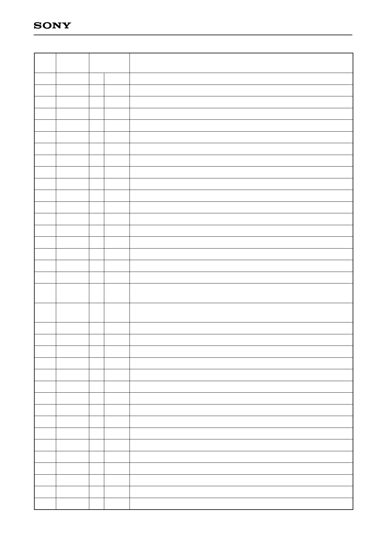
Pin
No.
Symbol
I/O
Description
36 BIAS
I
Constant current input of the asymmetry circuit.
37 ASYI
I
Asymmetry comparator voltage input.
38 ASYO
O 1, 0 EFM full-swing output (low = VSS, high = VDD).
39 LRCK
O 1, 0 D/A interface. LR clock output f = Fs.
40 LRCKI
I
LR clock input.
41 PCMD O 1, 0 D/A interface. Serial data output (two's complement, MSB first).
42 PCMDI I
D/A interface. Serial data input (two's complement, MSB first).
43 BCK
O 1, 0 D/A interface. Bit clock output.
44 BCKI
I
D/A interface. Bit clock input.
45 VSS
— — GND
46 VDD
47 XUGF
— — Power supply (+5V).
O 1, 0 XUGF output. Switched to MNT1 or RFCK output by a command.
48 XPCK
O 1, 0 XPLCK output. Switched to MNT0 output by a command.
49 GFS
O 1, 0 GFS output. Switched to MNT3 or XRAOF output by a command.
50 C2PO
O 1, 0 C2PO output. Switched to GTOP output by a command.
51 XTSL
I
Crystal selector input. Low: 16.9344MHz; high: 33.8688MHz.
52 C4M
O 1, 0 4.2336MHz output. 1/4 frequency-divided VCKI output in CAV-W mode.
53 DOUT O 1, 0 Digital Out output.
54 EMPH
Outputs a high signal when the playback disc has emphasis, and a low
O 1, 0 signal when there is no emphasis.
55 EMPHI I
Inputs a high signal when de-emphasis is on, and a low signal when
de-emphasis is off.
56 WFCK O 1, 0 WFCK output.
57 SCOR O 1, 0 Outputs a high signal when either subcode sync S0 or S1 is detected.
58 SBSO O 1, 0 Sub P to W serial output.
59 EXCK
I
SBSO readout clock input.
60 VSS
— — GND
61 VDD
62 SYSM
— — Power supply (+5V).
I
Mute input. Active when high.
63 AVSS
64 AVDD
— — Analog GND.
— — Analog power supply (+5V).
65 AOUT1 O
Left-channel analog output.
66 AIN1
I
Left-channel operational amplifier input.
67 LOUT1 O
Left-channel LINE output.
68 AVSS
69 XVDD
— — Analog GND.
Power supply for master clock.
70 XTAI
I
Crystal oscillation circuit input. Input the external master clock via this pin.
71 XTAO O
Crystal oscillation circuit output.
–5–
Share Link: 