7C1325-100(2000) View Datasheet(PDF) - Cypress Semiconductor
Part Name
Description
Manufacturer
7C1325-100 Datasheet PDF : 16 Pages
| |||
CY7C1325
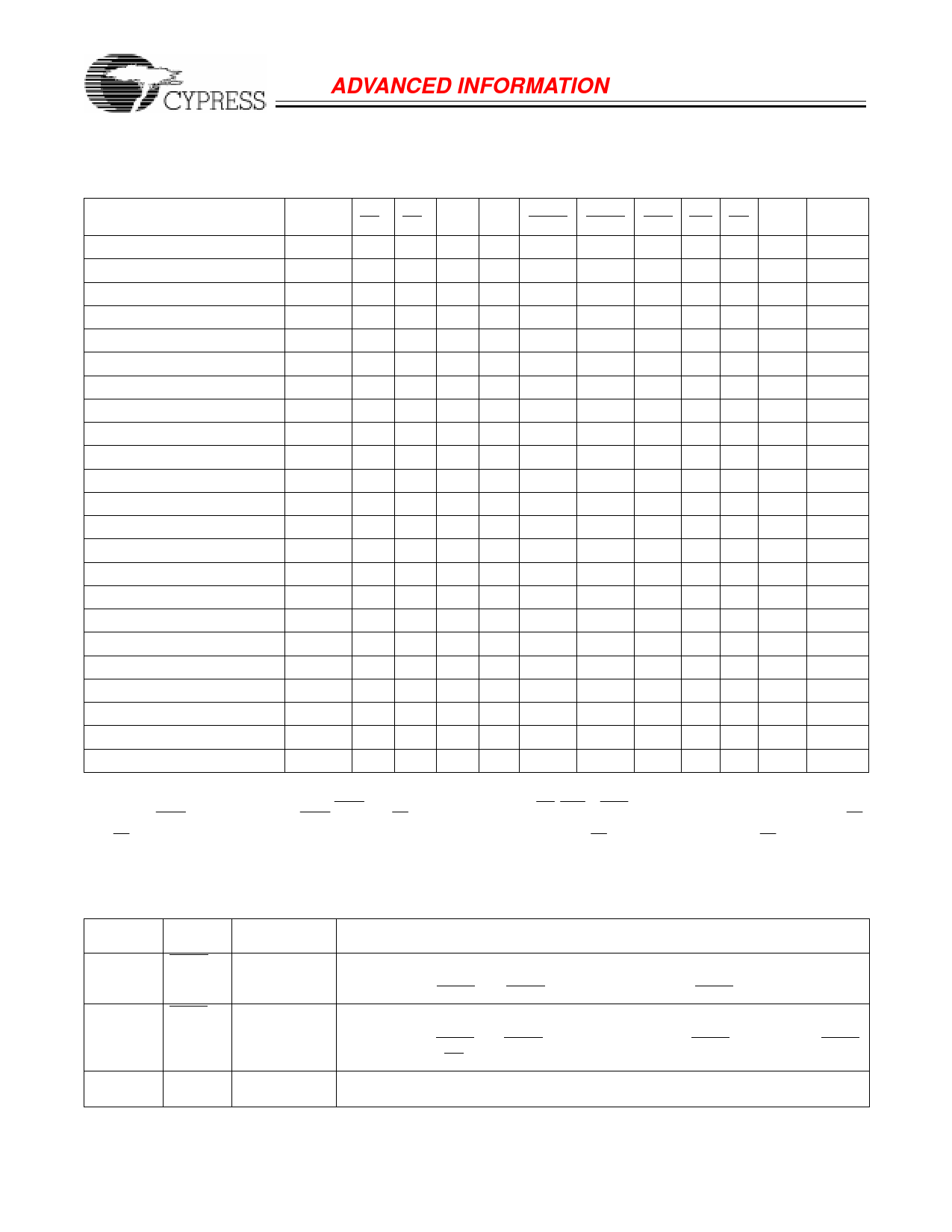
Pin Descriptions (continued)
Pin Number Name
5, 10, 17, 21, VSS
26, 40, 55,
60, 67, 71,
76, 90
4, 11, 20, 27, VDDQ
54, 61, 70,
77
1–3, 6, 7, 14, NC
16, 25,
28–30,
51–53, 56,
57, 66, 75,
78, 79,
95–96
38, 39, 42, DNU
43
I/O
Ground
I/O Power
Supply
-
-
Description
Ground for the device. Should be connected to ground of the system.
Power supply for the I/O circuitry. Should be connected to a 2.5 or 3.3V power supply.
No connects.
Do not use pins. Should be left unconnected or tied LOW.
Functional Overview
All synchronous inputs pass through input registers controlled
by the rising edge of the clock. Maximum access delay from
the clock rise (t CDV) is 7.5 ns (117-MHz device).
The CY7C1325 supports secondary cache in systems utilizing
either a linear or interleaved burst sequence. The interleaved
burst order supports Pentium and i486 processors. The linear
burst sequence is suited for processors that utilize a linear
burst sequence. The burst order is user selectable, and is de-
termined by sampling the MODE input. Accesses can be initi-
ated with either the processor address strobe (ADSP) or the
controller address strobe (ADSC). Address advancement
through the burst sequence is controlled by the ADV input. A
two-bit on-chip wraparound burst counter captures the first ad-
dress in a burst sequence and automatically increments the
address for the rest of the burst access.
Byte write operations are qualified with the Byte Write Enable
(BWE) and Byte Write Select (BWS[1:0]) inputs. A Global Write
Enable (GW) overrides all byte write inputs and writes data to
all four bytes. All writes are simplified with on-chip synchro-
nous self-timed write circuitry.
Three synchronous chip selects (CE1, CE2, CE3) and an asyn-
chronous output enable (OE) provide for easy bank selection
and output three-state control. ADSP is ignored if CE1 is
HIGH.
Single Read Accesses
A single read access is initiated when the following conditions
are satisfied at clock rise: (1) CE1, CE2, and CE3 are all as-
serted active, and (2) ADSP or ADSC is asserted LOW (if the
access is initiated by ADSC, the write inputs must be deassert-
ed during this first cycle). The address presented to the ad-
dress inputs is latched into the address register and the burst
counter/control logic and presented to the memory core. If the
OE input is asserted LOW, the requested data will be available
at the data outputs a maximum to tCDV after clock rise. ADSP
is ignored if CE1 is HIGH.
Single Write Accesses Initiated by ADSP
This access is initiated when the following conditions are sat-
isfied at clock rise: (1) CE1, CE2, and CE3 are all asserted
active, and (2) ADSP is asserted LOW. The addresses pre-
sented are loaded into the address register and the burst
counter/control logic and delivered to the RAM core. The write
inputs (GW, BWE, and BWS[1:0]) are ignored during this first
clock cycle. If the write inputs are asserted active (see Write
Cycle Descriptions table for appropriate states that indicate a
write) on the next clock rise, the appropriate data will be
latched and written into the device. Byte writes are allowed.
During byte writes, BWS0 controls DQ[7:0] and DP0 while
BWS1 controls DQ[15:8] and DP1. All I/Os are three-stated dur-
ing a byte write. Since these are common I/O device, the asyn-
chronous OE input signal must be deasserted and the I/Os
must be three-stated prior to the presentation of data to
DQ[15:0] and DP[1:0]. As a safety precaution, the data lines are
three-stated once a write cycle is detected, regardless of the
state of OE.
Single Write Accesses Initiated by ADSC
This write access is initiated when the following conditions are
satisfied at clock rise: (1) CE1, CE2, and CE3 are all asserted
active, (2) ADSC is asserted LOW, (3) ADSP is deasserted
HIGH, and (4) the write input signals (GW, BWE, and BWS[1:0])
indicate a write access. ADSC is ignored if ADSP is active LOW.
The addresses presented are loaded into the address register,
burst counter/control logic and delivered to the RAM core. The
information presented to DQ[15:0] and DP[1:0] will be written
into the specified address location. Byte writes are allowed,
with BWS0 controlling DQ[7:0] and DP0 while BWS1 controlling
DQ[15:8] and DP1. All I/Os are three-stated when a write is
detected, even a byte write. Since these are common I/O de-
vice, the asynchronous OE input signal must be deasserted
and the I/Os must be three-stated prior to the presentation of
data to DQ[15:0] and DP[1:0]. As a safety precaution, the data
lines are three-stated once a write cycle is detected, regard-
less of the state of OE.
4
Share Link: 