7C1325-100 View Datasheet(PDF) - Cypress Semiconductor
Part Name
Description
Manufacturer
7C1325-100 Datasheet PDF : 13 Pages
| |||
ADVANCED INFORMATION
CY7C1325
256K x 18 Synchronous
3.3V Cache RAM
Features
Functional Description
• Supports 117-MHz microprocessor cache systems with
zero wait states
• 256K by 18 common I/O
• Low Standby Power (6.6 mW, L version)
• Fast clock-to-output times
— 7.5 ns (117-MHz version)
• Two-bit wrap-around counter supporting either inter-
leaved or linear burst sequence
• Separate processor and controller address strobes pro-
vides direct interface with the processor and external
cache controller
• Synchronous self-timed write
• Asynchronous output enable
• I/Os capable of 2.5–3.3V operation
• JEDEC-standard pinout
• 100-pin TQFP packaging
• ZZ “sleep” mode
The CY7C1325 is a 3.3V 256K by 18 synchronous cache RAM
designed to interface with high-speed microprocessors with
minimum glue logic. Maximum access delay from clock rise is
7.5 ns (117-MHz version). A 2-bit on-chip counter captures the
first address in a burst and increments the address automati-
cally for the rest of the burst access.
The CY7C1325 allows both an interleaved or linear burst se-
quences, selected by the MODE input pin. A HIGH selects an
interleaved burst sequence, while a LOW selects a linear burst
sequence. Burst accesses can be initiated with the processor
address strobe (ADSP) or the cache controller address strobe
(ADSC) inputs. Address advancement is controlled by the ad-
dress advancement (ADV) input.
A synchronous self-timed write mechanism is provided to sim-
plify the write interface. A synchronous chip enable input and
an asynchronous output enable input provide easy control for
bank selection and output three-state control.
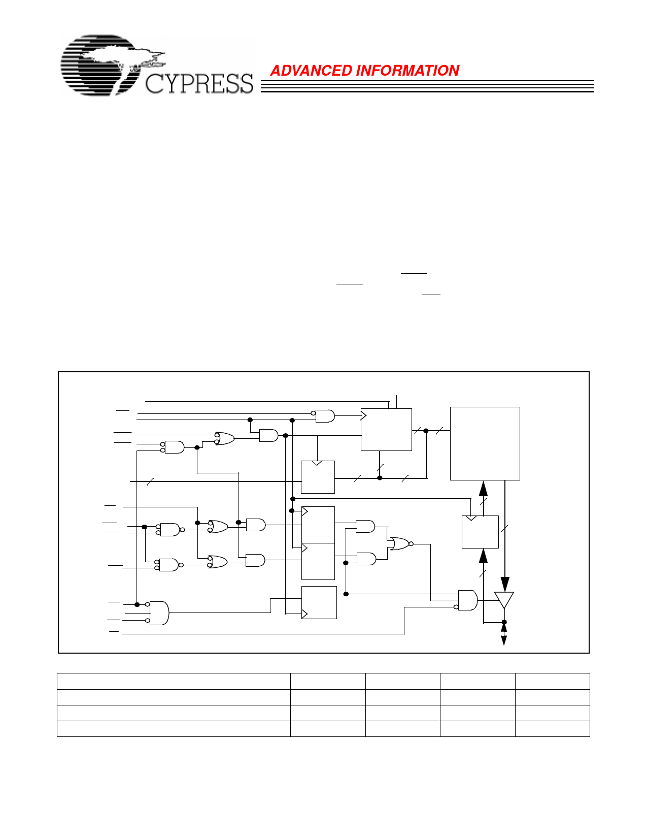
Logic Block Diagram
ZZ
MODE
ADV
CLK
ADSC
ADSP
BURST
2
COUNTER
CLR CONTROL
LOGIC
18
256KX18
MEMORY
ARRAY
ADDR<17:0>
18
GW
BWE
BWS1
ADDR
REG
2
18
16
UPPER
WRITE
REG
18
DATA-IN
18
REG
BWS0
LOWER
WRITE
REG
18
CE1
CE2
CE3
OE
ENABLE
REG
Selection Guide
Maximum Access Time (ns)
Maximum Operating Current (mA)
Maximum Standby Current (mA)
Pentium is a registered trademark of Intel Corporation.
7C1325–117
7.5
350
2.0
7C1325–100
8.0
325
2.0
DQ[15:0]
DP[1:0]
7C1325–80
8.5
300
2.0
7C1325–50
11.0
250
2.0
Cypress Semiconductor Corporation • 3901 North First Street • San Jose • CA 95134 • 408-943-2600
October 15, 1997
Share Link: 