7C1325-100 View Datasheet(PDF) - Cypress Semiconductor
Part Name
Description
Manufacturer
7C1325-100 Datasheet PDF : 13 Pages
| |||
ADVANCED INFORMATION
CY7C1325
Functional Description (continued)
Single Write Accesses Initiated by ADSP
This access is initiated when the following conditions are sat-
isfied at clock rise: (1) CE1, CE2, and CE3 are all asserted
active, and (2) ADSP is asserted LOW. The addresses pre-
sented are loaded into the address register and the burst
counter/control logic and delivered to the RAM core. The write
inputs (GW, BWE, and BWS[1:0]) are ignored during this first
clock cycle. If the write inputs are asserted active (see write
table for appropriate states that indicate a write) on the next
clock rise, the appropriate data will be latched and written into
the device. Byte writes are allowed. During byte writes, BWS0
controls DQ[7:0] and DP0 while BWS1 controls DQ[15:8] and
DP1. All I/Os are three-stated during a byte write. Since these
are common I/O device, the asynchronous OE input signal
must be deasserted and the I/Os must be three-stated prior to
the presentation of data to DQ[15:0] and DP[1:0]. As a safety
precaution, the data lines are three-stated once a write cycle
is detected, regardless of the state of OE.
Single Write Accesses Initiated by ADSC
This write access is initiated when the following conditions are
satisfied at clock rise: (1) CE1, CE2, and CE3 are all asserted
active, (2) ADSC is asserted LOW, (3) ADSP is deasserted
HIGH, and (4) The write input signals (GW, BWE, and
BWS[1:0]) indicate a write access. ADSC is ignored if ADSP is
active LOW.
The addresses presented are loaded into the address register,
burst counter/control logic and delivered to the RAM core. The
information presented to DQ[15:0] and DP[1:0] will be written
into the specified address location. Byte writes are allowed,
with BWS0 controlling DQ[7:0] and DP0 while BWS1 controlling
DQ[15:8] and DP1. All I/Os are three-stated when a write is
detected, even a byte write. Since these are common I/O de-
vice, the asynchronous OE input signal must be deasserted
and the I/Os must be three-stated prior to the presentation of
data to DQ[15:0] and DP[1:0]. As a safety precaution, the data
lines are three-stated once a write cycle is detected, regard-
less of the state of OE.
Single Read Accesses
A single read access is initiated when the following conditions
are satisfied at clock rise: (1) CE1, CE2, and CE3 are all as-
serted active, and (2) ADSP or ADSC is asserted LOW (if the
access is initiated by ADSC, the write inputs must be deassert-
ed during this first cycle). The address presented to the ad-
dress inputs is latched into the Address Register, burst counter
/control logic and presented to the memory core. If the OE
input is asserted LOW, the requested data will be available at
the data outputs a maximum to TCDV after clock rise. ADSP is
ignored if CE1 is HIGH.
Burst Sequences
This family of devices provide a 2-bit wrap around burst
counter inside the SRAM. The burst counter is fed by A[1:0],
and can follow either a linear or interleaved burst order. The
burst order is determined by the state of the MODE input. A
LOW on MODE will select a linear burst sequence. A HIGH on
MODE will select an interleaved burst order. Leaving MODE
unconnected will cause the device to default to a interleaved
burst sequence.
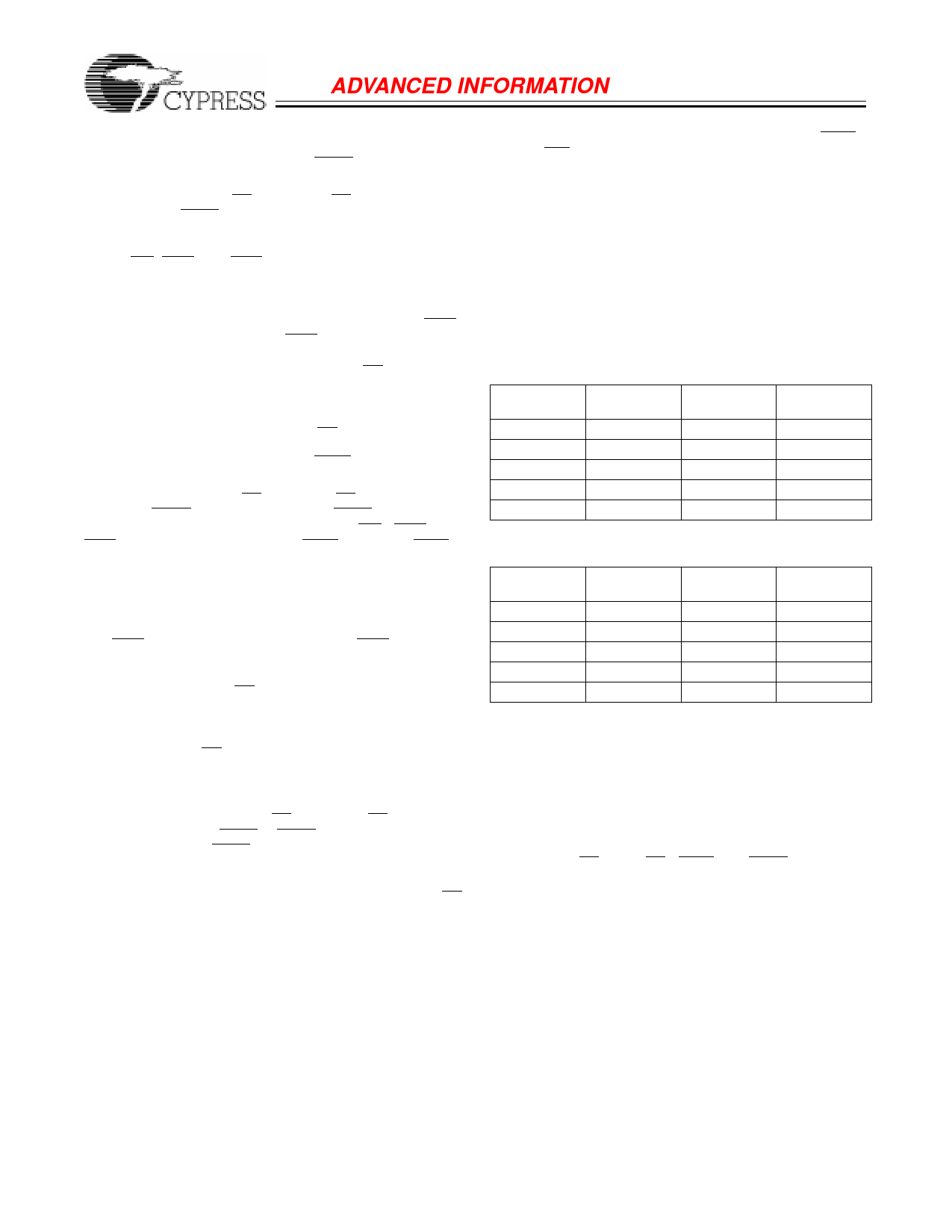
Table 1. Counter Implementation for the Intel
Pentium®/80486 Processor’s Sequence
First
Address
AX + 1, Ax
00
01
10
11
Second
Address
AX + 1, Ax
01
00
11
10
Third
Address
AX + 1, Ax
10
11
00
01
Fourth
Address
AX + 1, Ax
11
10
01
00
Table 2. Counter Implementation for a Linear Sequence
First
Address
AX + 1, Ax
00
01
10
11
Second
Address
AX + 1, Ax
01
10
11
00
Third
Address
AX + 1, Ax
10
11
00
01
Fourth
Address
AX + 1, Ax
11
00
01
10
Sleep Mode
The ZZ input pin is an asynchronous input. Asserting ZZ HIGH
places the SRAM in a power conservation “sleep” mode. Two
clock cycles are required to enter into or exit from this “sleep”
mode. While in this mode, data integrity is guaranteed. Ac-
cesses pending when entering the “sleep” mode are not con-
sidered valid nor is the completion of the operation guaran-
teed. The device must be deselected prior to entering the
“sleep” mode. CE1, CE2, CE3, ADSP, and ADSC must remain
inactive for the duration of tZZREC after the ZZ input returns
LOW.
3
Share Link: 