7C1325-100 View Datasheet(PDF) - Cypress Semiconductor
Part Name
Description
Manufacturer
7C1325-100 Datasheet PDF : 13 Pages
| |||
ADVANCED INFORMATION
CY7C1325
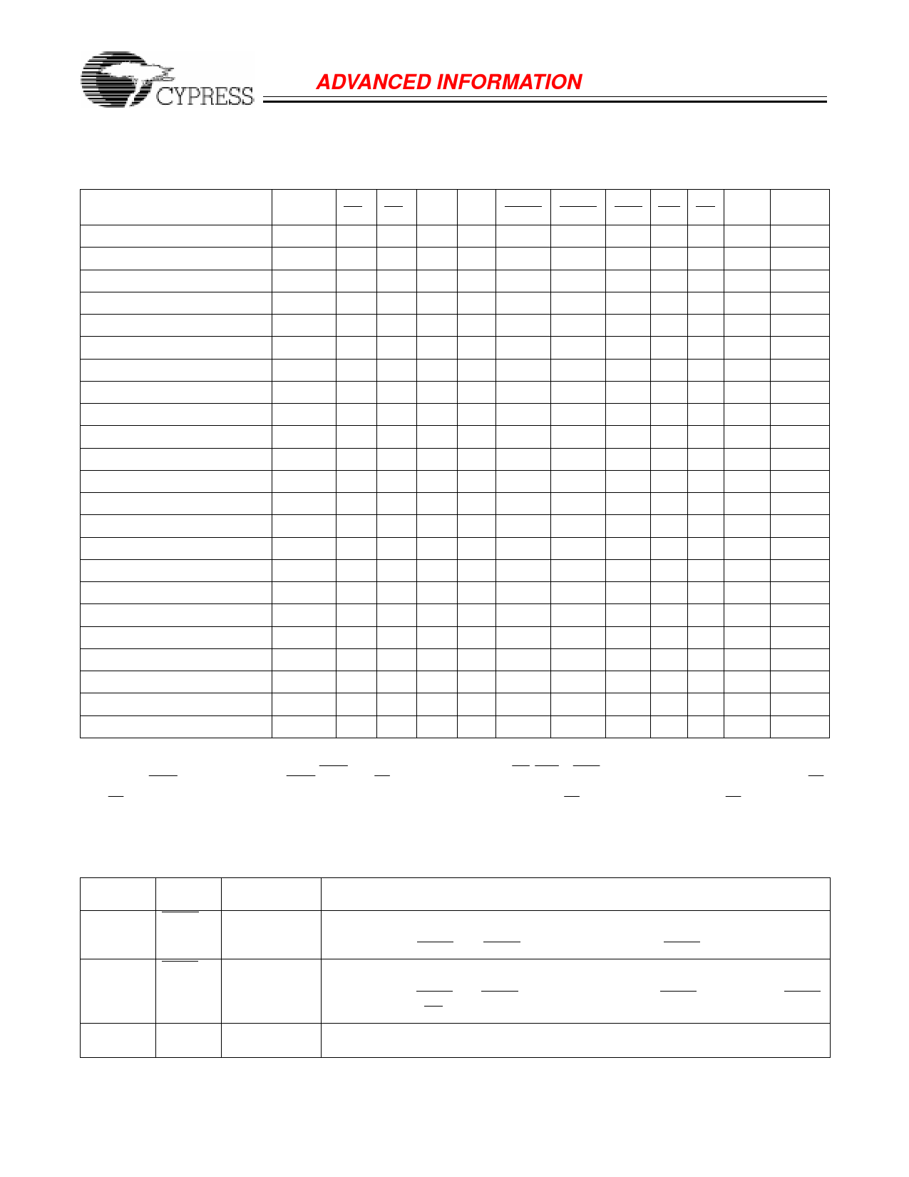
Cycle Description Table[1, 2, 3]
Cycle Description
Deselected Cycle, Power-down
ADD
Used
None
CE1 CE3 CE2 ZZ ADSP ADSP ADV WE OE CLK DQ
HXXL
X
L
X X X L-H HIGH-Z
Deselected Cycle, Power-down None L X L L
L
X
X X X L-H HIGH-Z
Deselected Cycle, Power-down None L H X L
L
X
X X X L-H HIGH-Z
Deselected Cycle, Power-down None L X L L
H
L
X X X L-H HIGH-Z
Deselected Cycle, Power-down None X X X L
H
L
X X X L-H HIGH-Z
SNOOZE MODE, Power-Down None X X X H
X
X
X X X X HIGH-Z
READ Cycle, Begin Burst
External L L H L
L
X
X X L L-H Q
READ Cycle, Begin Burst
External L L H L
L
X
X X H L-H HIGH-Z
WRITE Cycle, Begin Burst
External L L H L
H
L
X L X L-H D
READ Cycle, Begin Burst
External L L H L
H
L
X H L L-H Q
READ Cycle, Begin Burst
External L L H L
H
L
X H H L-H HIGH-Z
READ Cycle, Continue Burst
Next
XXXL
H
H
L H L L-H Q
READ Cycle, Continue Burst
Next
XXXL
H
H
L H H L-H HIGH-Z
READ Cycle, Continue Burst
Next H X X L
X
H
L H L L-H Q
READ Cycle, Continue Burst
Next H X X L
X
H
L H H L-H HIGH-Z
WRITE Cycle, Continue Burst Next
XXXL
H
H
L L X L-H D
WRITE Cycle, Continue Burst Next
HXXL
X
H
L L X L-H D
READ Cycle, Suspend Burst Current X X X L
H
H
H H L L-H Q
READ Cycle, Suspend Burst Current X X X L
H
H
H H H L-H HIGH-Z
READ Cycle, Suspend Burst Current H X X L
X
H
H H L L-H Q
READ Cycle, Suspend Burst Current H X X L
X
H
H H H L-H HIGH-Z
WRITE Cycle, Suspend Burst Current X X X L
H
H
H L X L-H D
WRITE Cycle, Suspend Burst Current H X X L
X
H
H L X L-H D
Notes:
1. X=Don't Care, 1=Logic HIGH, 0=Logic LOW.
2. The SRAM always initiates a read cycle when ADSP asserted, regardless of the state of GW, BWE, or BWS[1:0]. Writes may occur only on subsequent clocks
after the ADSP or with the assertion of ADSC. As a result, OE must be driven HIGH prior to the start of the write cycle to allow the outputs to three– state. OE
is a don't care for the remainder of the write cycle.
3. OE is asynchronous and is not sampled with the clock rise. During a read cycle DQ=HIGH–Z when OE is inactive, and DQ=data when OE is active
Pin Descriptions
TQFP Pin
Number Name
85
ADSC
84
ADSP
36, 37
A[1:0]
I/O
Input-
Synchronous
Input-
Synchronous
Input-
Synchronous
Description
Address Strobe from Controller, sampled on the rising edge of CLK. When asserted
LOW, A[17:0] is captured in the address registers. A[1:0] are also loaded into the burst
counter. When ADSP and ADSC are both asserted, only ADSP is recognized.
Address Strobe from Processor, sampled on the rising edge of CLK. When asserted
LOW, A[17:0] is captured in the address registers. A[1:0] are also loaded into the burst
counter. When ADSP and ADSC are both asserted, only ADSP is recognized. ASDP
is ignored when CE1 is deasserted HIGH.
A1, A0 address inputs, These inputs feed the on-chip burst counter as the LSBs as
well as being used to access a particular memory location in the memory array.
4
Share Link: 