7C1325-100 View Datasheet(PDF) - Cypress Semiconductor
Part Name
Description
Manufacturer
7C1325-100 Datasheet PDF : 13 Pages
| |||
ADVANCED INFORMATION
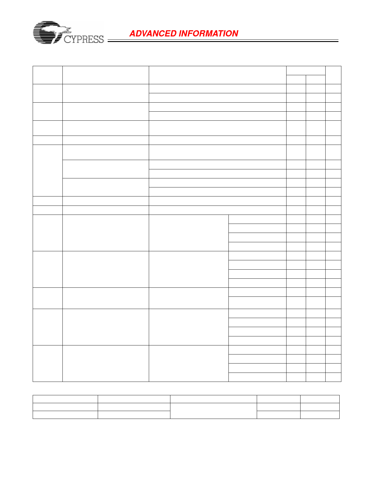
CY7C1325
Electrical Characteristics Over the Operating Range
7C1325
Parameter
Description
Test Conditions
Min. Max. Unit
VOH
Output HIGH Voltage
VOL
Output LOW Voltage
VIH
Input HIGH Voltage
VIL
Input LOW Voltage[5]
IX
Input Load Current
(except ZZ and MODE)
VDDQ = 3.3V, VDD = Min., IOH=–4.0 mA
VDDQ = 2.5V, VDD = Min., IOH=–2.0 mA
VDDQ = 3.3V, VDD = Min., IOL=8.0 mA
VDDQ = 2.5V, VDD = Min., IOL=2.0 mA
GND ≤ VI ≤ VDDQ
2.4
V
1.7
V
0.4 V
0.7 V
1.7 VDD + V
0.3V
–0.3 0.8 V
−1
1 µA
Input Current of MODE
Input = VSS
–30
µA
Input = VDDQ
5 µA
Input Current of ZZ
Input = VSS
–5
µA
Input = VDDQ
30 µA
IOZ
Output Leakage Current
GND ≤ VI ≤ VDD, Output Disabled
IOS
Output Short Circuit Current[7]
VDD=Max., VOUT=GND
–5
5 µA
–300 mA
IDD
VDD Operating Supply Current
VDD=Max., Iout=0mA,
f=fMAX =1/tCYC.
8.5 ns cycle, 117 MHz
10 ns cycle, 100 MHz
350 mA
325 mA
11 ns cycle, 90 MHz
300 mA
20 ns cycle,50 MHz
250 mA
ISB1
Automatic CE Power-Down
Max. VDD, Device Deselected, 8.5 ns cycle, 117 MHz
Current—TTL Inputs switching
VIN ≥ VIH or VIN ≤ VIL, f=fMAX,
inputs switching
10 ns cycle, 100 MHz
11 ns cycle, 90 MHz
125 mA
110 mA
100 mA
20 ns cycle,50 MHz
75 mA
ISB2
Automatic CE Power-Down
Max. VDD, Device Deselected, Std version -All speeds
Current — CMOS Inputs static
VIN ≥ VDD –0.3V or VIN ≤ 0.3V,
f=0, inputs static
L version -All speeds
10 mA
2 mA
ISB3
Automatic CE Power-Down
Max. VDD, Device Deselected, 8.5 ns cycle, 117 MHz
Current—CMOS Inputs switching,
F=Max
VIN ≥ VDDQ– 0.3V or VIN ≤ 0.3V,
f=fMAX, inputs switching
10 ns cycle, 100MHz
11 ns cycle, 90MHz
95 mA
85 mA
70 mA
20 ns cycle,50MHz
60 mA
ISB4
Automatic CE Power-Down Current Max. VDD, Device Deselected, 8.5 ns cycle, 117 MHz
— CMOS Inputs static, F=Max
VIN ≥ VDD –0.3V or VIN ≤ 0.3V,
f=fMAX, inputs static
10 ns cycle, 100MHz
11 ns cycle, 90MHz
60 mA
50 mA
40 mA
20 ns cycle,50MHz
35 mA
Capacitance[8]
Parameter
Description
Test Conditions
CIN
Input Capacitance
TA = 25°C, f = 1 MHz,
CI/O
I/O Capacitance
VDD = 5.0V
Notes:
7. Not more than one output should be shorted at one time. Duration of the short circuit should not exceed 30 seconds.
8. Tested initially and after any design or process changes that may affect these parameters
Max.
5.0
8.0
Unit
pF
pF
8
Share Link: 