MCM64PD64SG66 View Datasheet(PDF) - Motorola => Freescale
Part Name
Description
Manufacturer
MCM64PD64SG66 Datasheet PDF : 16 Pages
| |||
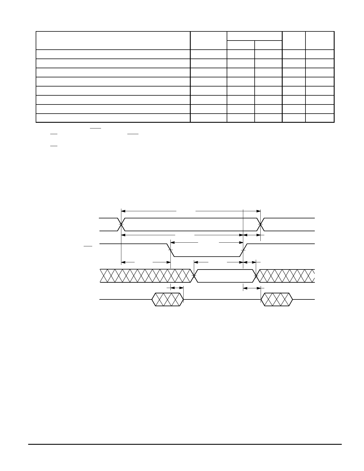
TAG RAM WRITE CYCLE (See Notes 1 and 2)
– 15
Parameter
Symbol
Min
Max
Unit
Notes
Write Cycle Time
tAVAV
15
—
ns
3
Address Setup Time
tAVWL
0
—
ns
Address Valid to End of Write
tAVWH
12
—
ns
Data Valid to End of Write
tDVWH
7
—
ns
Data Hold Time
tWHDX
0
—
ns
Write Low to Output High–Z
tWLQZ
0
7
ns
5,6,7
Write High to Output Active
tWHQX
4
—
ns
5,6,7
Write Recovery Time
tWHAX
0
—
ns
NOTES:
1. A write occurs when CWE is low.
2. If CG goes low coincident with or after CWE goes low, the output will remain in a high impedance state.
3. All timings are referenced from the last valid address to the first address transition.
4. If CG ≥ VIH, the output will remain in a high impedance state.
5. At any given voltage and temperature, tWLQZ (max) is less than tWHQX (min), both for a given device and from device to device.
6. Transition is measured ±500 mV from steady–state voltage with load of Figure 3B.
7. This parameter is sampled and not 100% tested.
AX (ADDRESS)
TWE
D (DATA IN)
Q (DATA OUT)
TAG RAM WRITE CYCLE (See Notes 1 and 2)
tAVAV
tAVWH
tWLWH
tAVWL
HIGH Z
tWLQZ
tDVWH
DATA VALID
HIGH Z
tWHAX
tWHDX
tWHQX
MOTOROLA FAST SRAM
MCM64PD32•MCM64PD64
13
Share Link: 