FIN1049 View Datasheet(PDF) - ON Semiconductor
Part Name
Description
Manufacturer
FIN1049 Datasheet PDF : 14 Pages
| |||
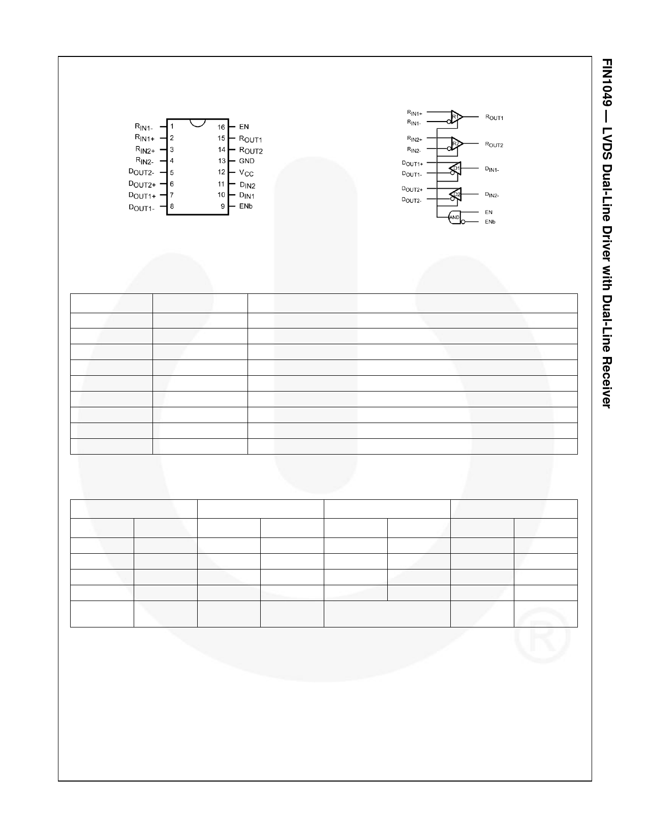
Pin Configuration
Functional Diagram
Figure 1. Pin Configuration
Figure 2. Functional Diagram
Pin Definitions
Pin #
2, 3
1, 4
7, 6
8, 5
16, 9
15, 14
10, 11
12
13
Name
RIN1+, RIN2+
RIN1-, RIN2-
DOUT1+, DOUT2+
DOUT1-, DOUT2-
EN, ENb
ROUT1, ROUT2
DIN1, DIN2
VCC
GND
Description
Non-Inverting LVDS Inputs
Inverting LVDS Inputs
Non-Inverting Driver Outputs
Inverting Driver Outputs
Driver Enable Pins for All Outputs
LVTTL Output Pins for ROUT1 and ROUT2
LVTTL Input Pins for DIN1 and DIN2
Power Supply (3.3 V)
Ground
Function Table
Inputs
EN
ENb
H
L
H
H
L
H
L
L
Outputs (LVTTL)
ROUT1
ON
Z
Z
Z
ROUT2
ON
Z
Z
Z
H
L
H
H
Legend:
H=HIGH Logic Level
L=LOW Logic Level or OPEN
X=Don't Care
Z=High Impedance
Note:
1. Any unused receiver Inputs should be left open.
Inputs (LVDS)(1)
RINn+
RINn-
Open Current
Fail-Safe Condition
Outputs (LVDS)
DOUTn+
ON
Z
Z
Z
DOUTn-
ON
Z
Z
Z
© 2003 Fairchild Semiconductor Corporation
FIN1049 • Rev. 1.0.3
2
www.fairchildsemi.com
Share Link: 