FIN1049 View Datasheet(PDF) - ON Semiconductor
Part Name
Description
Manufacturer
FIN1049 Datasheet PDF : 14 Pages
| |||
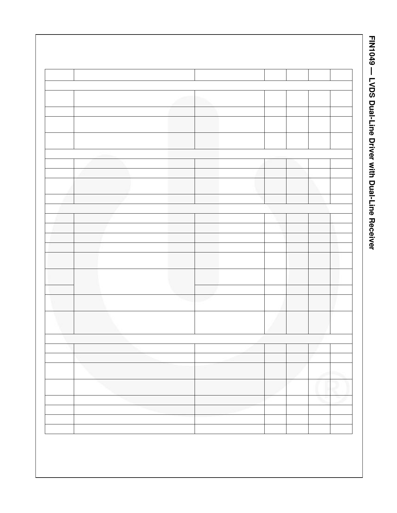
DC Electrical Characteristics
Over-supply voltage and operating temperature ranges, unless otherwise specified. All typical values are at TA=25°C
and with VCC=3.3 V.
Symbol
Parameter
Conditions
Min. Typ. Max. Units
LVDS Input DC Specifications (RIN1+, RIN1-, RIN2+, RIN2-) See Figure 3 and Table 1
VTH Differential Input Threshold HIGH
VCM=1.2 V, 0.05 V,
2.35 V
0
35 mV
VTL Differential Input Threshold LOW
VIC Common Mode Voltage Range
VID=100 mV, VCC=3.3 V
IIN Input Current
VCC=0 V or 3.6 V,
VIN=0 V or 2.8 V
CMOS/ LVTTL Input DC Specifications (EN, ENb, DIN1, DIN2)
VIH Input High Voltage (LVTTL)
VIL Input Low Voltage (LVTTL)
IIN
Input Current (EN, ENb, DIN1, DIN2, RINx+,
RINx-)
VIN=0 V or VCC
VIK Input Clamp Voltage
VIK=-18 mA
LVDS Output DC Specifications (DOUT1+, DOUT1-, DOUT2+, DOUT2-)
VOD Output Differential Voltage
See Figure 4
VOD VOD Magnitude Change from
RL=100
Differential LOW-to-HIGH
Driver Enabled
-100
VID/2
2.0
GND
-1.5
250
0
mV
VCC -
(VID/2)
V
±20 mA
VCC
V
0.8
V
±20 µA
-0.7
V
350 450 mV
35 mV
VOS
VOS
Offset Voltage
Offset Magnitude Change from Differential
LOW-to-HIGH
See Figure 4
1.125 1.250 1.375 V
25 mV
IOS
Short-Circuit Output Current
DOUT+=0V & DOUT-=0 V,
Driver Enabled
IOSD
VOD=0 V, Driver Enabled
IOFF Power-Off Input or Output Current
VCC=0 V, VOUT=0 V or
VCC
IOZD Disabled Output Leakage Current
Driver Disabled,
DOUT+=0 V or VCC or
DOUT-=0V or VCC
CMOS/LVTTL Output DC Specifications (ROUT1, ROUT2)
VOH Output High Voltage
IOH=-2 mA, VID=200 mV
2.7
VOL Output Low Voltage
IOL=2 mA, VID=200 mV
IOZ Disabled Output Leakage Current
Driver Disabled,
ROUTn=0 V or VCC
ICC
Power Supply Current(2)
Drivers Enabled, Any
Valid Input Condition
-9 mA
-9 mA
±20 mA
±10 mA
V
0.25 V
±10 mA
25 mA
ICCZ Power Supply Current
Drivers Disabled
10 mA
CIND Input Capacitance
LVDS Input
3.0
pF
COUT Output Capacitance
LVDS Output
4.0
pF
CINT Input Capacitance
LVTTL Input
3.5
pF
Note:
2. Both driver and receiver inputs are static. All LVDS outputs have 100 load. None of the outputs have any
lumped capacitive load.
© 2003 Fairchild Semiconductor Corporation
FIN1049 • Rev. 1.0.3
4
www.fairchildsemi.com
Share Link: 