FIN1049 View Datasheet(PDF) - ON Semiconductor
Part Name
Description
Manufacturer
FIN1049 Datasheet PDF : 14 Pages
| |||
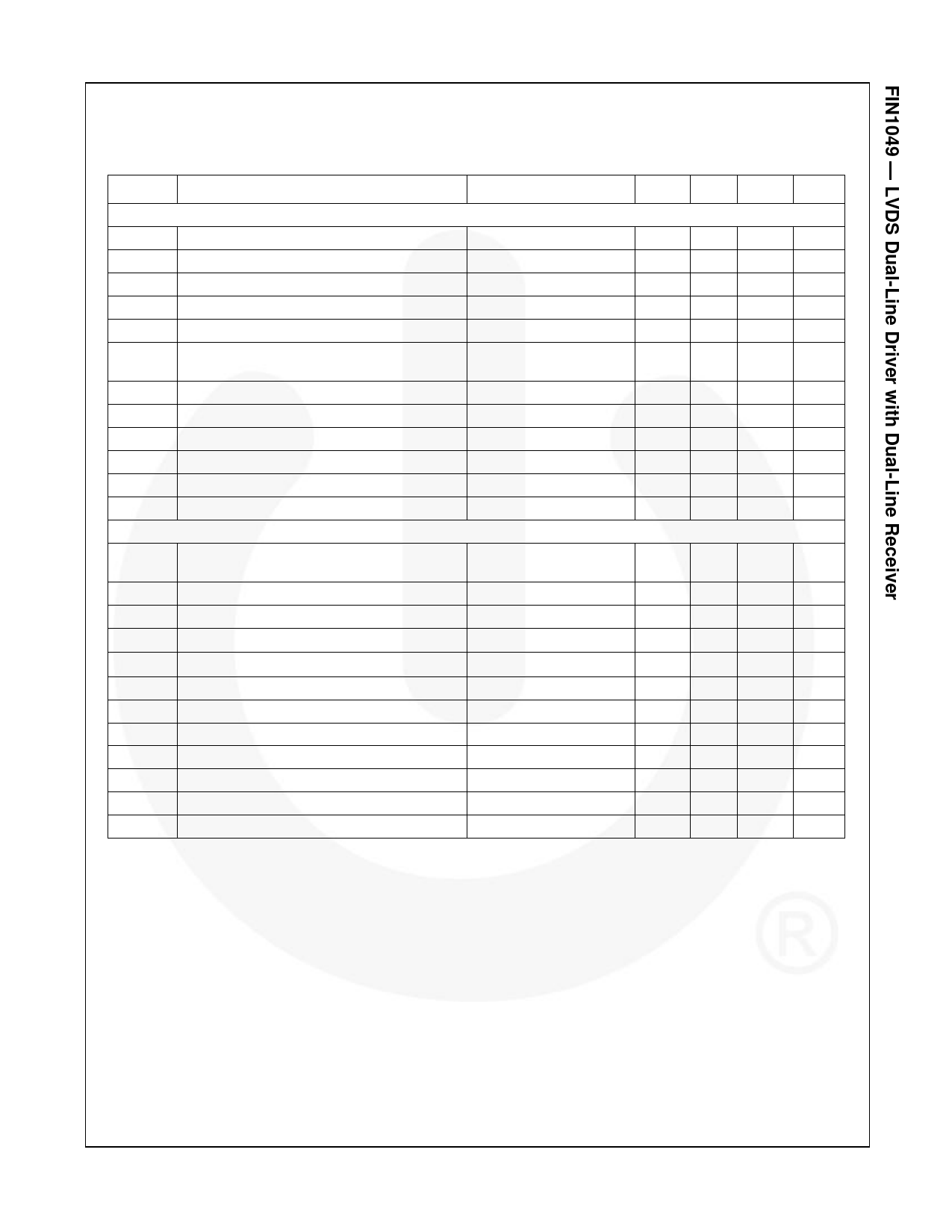
AC Electrical Characteristics
Over-supply voltage and operating temperature ranges, unless otherwise specified. All typical values are at TA=25°C
and with VCC=3.3 V.
Symbol
Parameter
Conditions
Min. Typ. Max. Units
Switching Characteristics - LVDS Outputs
tPLHD Differential Propagation Delay LOW-to-HIGH See Figure 5, Figure 6
tPHLD Differential Propagation Delay HIGH-to-LOW
tTLHD Differential Output Rise Time (20% to 80%)
0.2
tTHLD Differential Output Fall Time (80% to 20%)
0.2
tSK(P) Pulse Skew |tPLH - tPHL|
tSK(LH),
tSK(HL)
tSK(PP)
Channel-to-Channel Skew(3)
Part-to-Part Skew(4)
tPZHD Differential Output Enable Time, Z-to-HIGH See Figure 7, Figure 8
tPZLD Differential Output Enable Time, A-to-LOW
tPHZD Differential Output Disable Time, HIGH-to-Z
tPLZD Differential Output Disable Time, LOW-to-Z
fMAXD Maximum Frequency(5)
See Figure 5
200
Switching Characteristics - LVTTL Outputs
2
ns
2
ns
1.0
ns
1.0
ns
0.35 ns
0.35 ns
1
ns
6
ns
6
ns
3
ns
3
ns
MHz
tPHL Propagation Delay HIGH-to-LOW
Measured from 20% to
80% Signal
0.5 1.0 3.5
ns
tPLH Propagation Delay LOW-to-HIGH
VID=200 mV
0.5 1.0 3.5
ns
tSK1 Pulse Skew
Distributed Load
0
35 400 ps
tSK2 Channel-to-Channel Skew
CL=15 pF and 50
0
50 500 ps
tSK3 Part-to-Part Skew
RL=1 k
0
1
ns
tLHR Transition Time LOW-to-HIGH
VOS=1.2 V
0.10 0.25 1.40 ns
tHLR Transition Time HIGH-to-LOW
See Figure 9, Figure 10 0.10 0.18 1.40 ns
tPHZ Disable Time HIGH-to-Z
See Figure 11, Figure 12 2.2 4.5 8.0
ns
tPLZ Disable Time LOW-to-Z
1.3 3.5 8.0
ns
tPZH Enable Time Z-to-HIGH
1.8 3.0 7.0
ns
tPZL
fMAXT
Enable Time Z-to-LOW
Maximum Frequency(6)
See Figure 9
0.9 1.4
200
7.0
ns
MHz
Notes:
3. tSK(LH), tSK(HL) is the skew between specified outputs of a single device when the outputs have identical loads and
are switching in the same direction.
4. tSK(PP) is the magnitude of the difference in propagation delay times between any specified terminals of two
devices switching in the same direction (either LOW-to-HIGH or HIGH-to-LOW) when both devices operate with
the same supply voltage, same temperature, and have identical test circuits.
5. fMAXD generator input conditions: tr=tf < 1 ns (10% to 90%), 50% duty cycle, 0 V to 3 V. Output criteria: duty
cycle=45% / 55%, VOD > 250 mV, all channels switch.
6. fMAXT generator input conditions: tr=tf < 1 ns (10% to 90%), 50% duty cycle, VID=200 mV, VCM=1.2 V. Output
criteria: duty cycle=45% / 55%, VOH > 2.7 V. VOL < 0.25 V, all channels switching.
© 2003 Fairchild Semiconductor Corporation
FIN1049 • Rev. 1.0.3
5
www.fairchildsemi.com
Share Link: 