CXA3268AR View Datasheet(PDF) - Sony Semiconductor
Part Name
Description
Manufacturer
CXA3268AR Datasheet PDF : 42 Pages
| |||
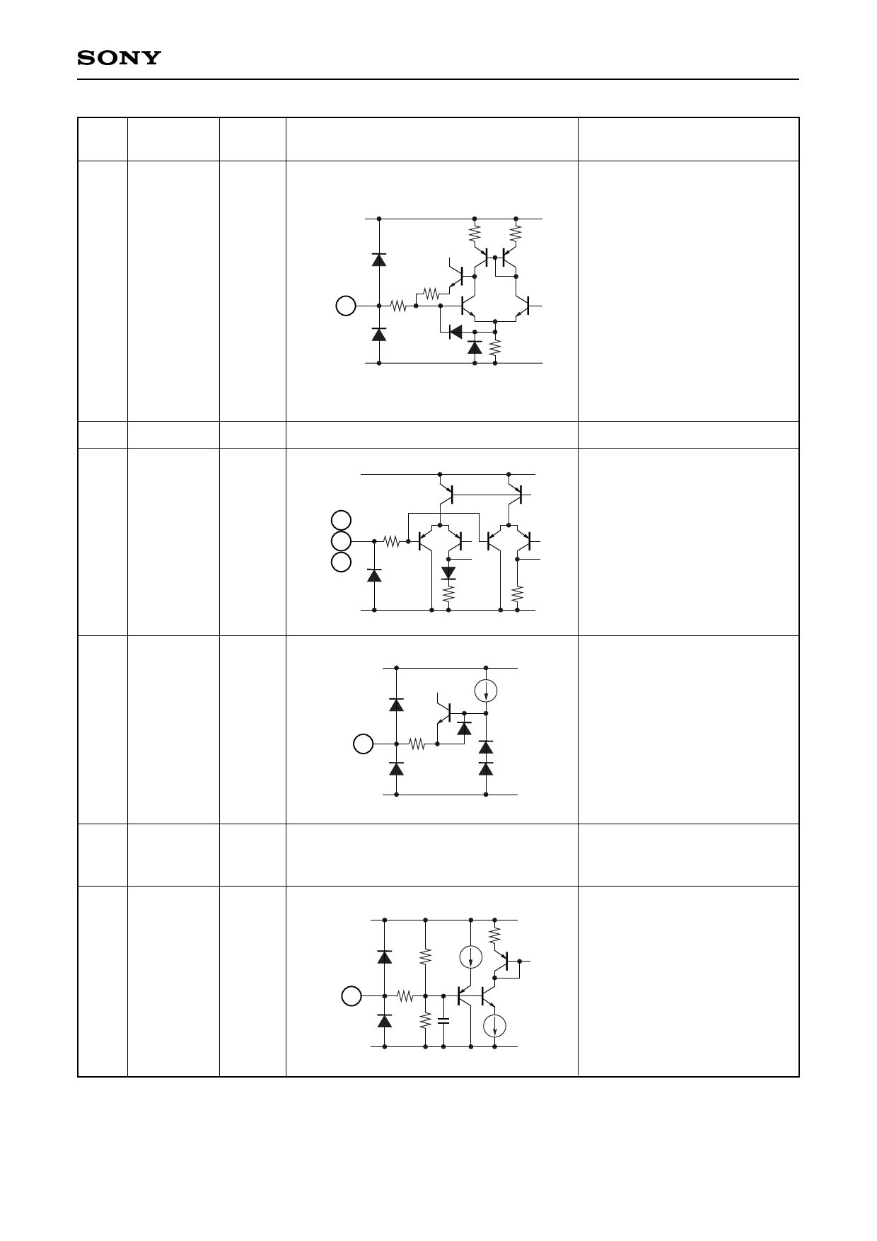
Pin
No.
Symbol
Pin
voltage
Equivalent circuit
8 F ADJ
1.1V
VCC1
6.5k
8
10
GND1
9 GND1
—
14 SCK
15 SEN
—
16 SDAT
17 R INJECT 0.7V
29 GND2
—
VCC1
14
15
200
16
GND1
VCC1
200
17
GND1
30 SIG.C
Preset
VCC2/2
Variable
range:
5.0 to 6.5V
VCC2
140k
30
GND1
200
140k 10p
–6–
CXA3268AR
Description
Connect a resistor between this
pin and GND1 to control the
internal LPF and trap
frequencies.
Connect a 33kΩ resistor
(tolerance ±2%, temperature
characteristics ±200ppm or less).
This pin is easily affected by
external noise, so make the
connection between the pin and
external resistor, and between
the GND side of the external
resistor and the GND1 pin as
close as possible.
Analog 3.0V GND.
Serial clock, serial load and
serial data inputs for serial
communication.
Connect a resistor for setting
the injector current of the IIL
logic circuit. Connect a 15kΩ
resistor between this pin and
GND1. Use a resistor with a
deviation of ±2% and
temperature characteristics of
±200ppm or less.
Analog 12.0V GND.
(for the RGB and PSIG output
circuits)
R, G, B and PSIG output DC
voltage setting.
Connect a 0.01µF capacitor
between this pin and GND1.
When using a SIG.C of other
than VCC2/2, input the SIG.C
voltage from an external
source.
Share Link: 