PBL3772-1 View Datasheet(PDF) - Ericsson
Part Name
Description
Manufacturer
PBL3772-1 Datasheet PDF : 8 Pages
| |||
PBL 3772/1
VBB2 5
E2 6
M B2 7
M B1 8
GND 9
E1 10
VBB1 11
PBL 3772/1QN
25 VR2
24 C2
23 RC
22 VCC
21 C1
20 VR1
19 Phase1
RC 1
22 VCC
C2 2
V R2 3
21 C1
20 VR1
Phase 2 4
19 Phase1
GND 5
GND 6
VMM2 7
PBL
3772/1N
18 GND
17 GND
16 VMM1
MA2 8
15 MA1
VBB2 9
14 VBB1
E2 10
MB2 11
13 E1
12 MB1
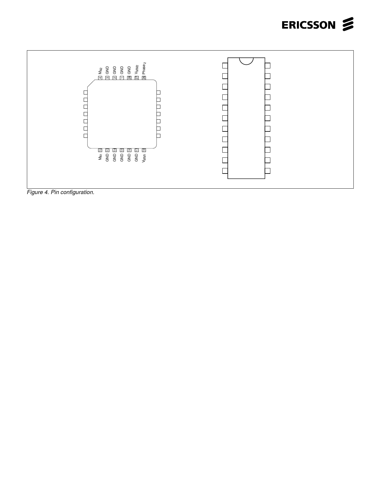
Figure 4. Pin configuration.
Pin Description
PLCC DIP
Symbol
1-3, 9, 5, 6 GND
13-17 17, 18
28
4
8
MA2
5
9
VBB2
6
10 E
2
7
11
MB2
8
12
MB1
10
13
E1
11
14
VBB1
12 15 M
A1
18 16 V
MM1
19
19
Phase1
20
20
VR1
21
21
C1
22
22
VCC
23 1
RC
24 2
C2
25 3
26 4
27 7
VR2
Phase2
VMM2
Description
Ground and negative supply. Note: these pins are used thermally for heat-sinking.
Make sure that all ground pins are soldered onto a suitably large copper ground
plane for efficient heat sinking.
Motor output A, channel 2. Motor current flows from MA2 to MB2 when Phase2 is HIGH.
Collector of upper output transistor, channel 2. For lowest possible power dissipation, connect a series
resistor RB2 to VMM2. See Applications information, External components.
Common emitter, channel 2. This pin connects to a sensing resistor R to ground.
S
Motor output B, channel 2. Motor current flows from MA2 to MB2 when Phase2 is HIGH.
Motor output B, channel 1. Motor current flows from MA1 to MB1 when Phase1 is HIGH.
Common emitter, channel 1. This pin connects to a sensing resistor RS to ground.
Collector of upper output transistor, channel 1. For lowest possible power dissipation, connect a series
resistor RB1 to VMM1. See Applications information, External components.
Motor output A, channel 1. Motor current flows from M to M when Phase is HIGH.
A1
B1
1
Motor supply voltage, channel 1, +10 to +40 V. V and V should be connected together.
MM1
MM2
Controls the direction of motor current at outputs MA1 and MB1. Motor current flows from MA1 to MB1
when Phase1 is HIGH.
Reference voltage, channel 1. Controls the threshold voltage for the comparator and hence the output
current.
Comparator input channel 1. This input senses the instantaneous voltage across the sensing resistor,
filtered by an RC network. The threshold voltage for the comparator is V = 0.18 • V [V], i.e. 450
CH1
R1
mV at VR1 = 2.5 V.
Logic voltage supply, nominally +5 V.
Clock oscillator RC pin. Connect a 15 kohm resistor to VCC and a 3300 pF capacitor to ground to
obtain the nominal switching frequency of 26.5 kHz.
Comparator input channel 2. This input senses the instantaneous voltage across the sensing resistor,
filtered by an RC network. The threshold voltage for the comparator is V = 0.18 • V [V], i.e. 450 mV
CH2
R2
at V = 2.5 V.
R2
Reference voltage, channel 2. Controls the threshold voltage for the comparator and hence the output
current.
Controls the direction of motor current at outputs MA2 and MB2. Motor current flows from MA2 to MB2
when Phase2 is HIGH.
Motor supply voltage, channel 2, +10 to +40 V.VMM1 and VMM2 should be connected together.
4
Share Link: 