2SK3539G View Datasheet(PDF) - Panasonic Corporation
Part Name
Description
Manufacturer
2SK3539G Datasheet PDF : 4 Pages
| |||
This product complies with the RoHS Directive (EU 2002/95/EC).
Silicon MOSFETs (Small Signal)
2SK3539G
Silicon N-channel MOSFET
For switching
■ Features
• High-speed switching
/ • Wide frequency band
• Gate protection diode built-in
ce tage. ■ Absolute Maximum Ratings Ta = 25°C
n d s Parameter
Symbol Rating
Unit
ycle Drain-source voltage
a e lifec Gate-source voltage (Drain open)
t Drain current
n u duc Peak drain current
Pro Power dissipation
te tin ur Channeltemperature
g fo e . Storage temperature
VDS
50
V
VGSO
±7
V
ID
100
mA
IDP
200
mA
PD
150
mW
Tch
150
°C
Tstg −55 to +150 °C
■ Package
• Code
SMini3-F2
• Marking Symbol: 5F
• Pin Name
1: Gate
2: Source
3: Drain
in nes follotweninancettyyppe typed formatio/n ■ Electrical Characteristics Ta = 25°C ± 3°C
a o lud in ce d t in /en Parameter
Symbol
Conditions
Min Typ Max Unit
c ed inc ed ma tenan tinue type tes .jp Drain-source surrender voltage
M is tinu lan ain con ed ut la ic.co Drain-source cutoff current
p m dis tinu bo on Gate-Source cutoff current
on d n a as Gate threshold voltage
isc lane isco URL .pan Drain-source ON resistance
D ce/D p d wing icon Forward trancfer admitance
tenan follo .sem Short-circuit forward transfer
in it w capacitance (Common source)
VDSS
IDSS
IGSS
Vth
RDS(on)
Yfs
Ciss
ID = 10 µA, VGS = 0
VDS = 50 V, VGS = 0
VGS = ±7 V, VDS = 0
ID = 1.0 µA, VDS = 3 V
ID = 10 mA, VGS = 2.5 V
ID = 10 mA, VGS = 4.0 V
ID = 10 mA, VDS = 3 V, f = 1 kHz
VDS = 3 V, VGS = 0, f = 1 MHz
50
V
1.0
µA
±5.0 µA
0.9 1.2 1.5
V
8
15
Ω
6
12
20 60
mS
12
pF
Ma e vis ://ww Short-circuit output capacitance (Common source)
Coss
7
pF
as ttp Reverse transfer capacitance (Common source) Crss
3
pF
Ple h Turn-on time *
ton
VDD = 3 V, VGS = 0 V to 3 V, RL = 470 Ω
200
ns
Turn-off time *
toff
VDD = 3 V, VGS = 3 V to 0 V, RL = 470 Ω
200
ns
Note) 1. Measuring methods are based on JAPANESE INDUSTRIAL STANDARD JIS C 7030 measuring methods for transistors.
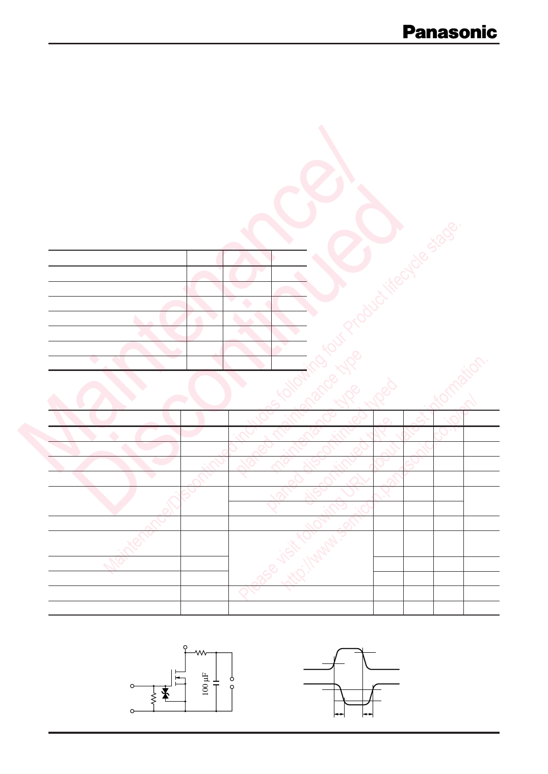
2. *: ton , toff test circuit
VOUT 470 Ω
90%
VGS = 3.0 V
50 Ω
VDD = 3 V
VIN
VOUT
10%
10%
90%
ton
toff
Publication date: June 2007
SJF00068AED
1
Share Link: 