ICL7126 View Datasheet(PDF) - Renesas Electronics
Part Name
Description
Manufacturer
ICL7126 Datasheet PDF : 15 Pages
| |||
ICL7216
Detailed Description
Analog Section
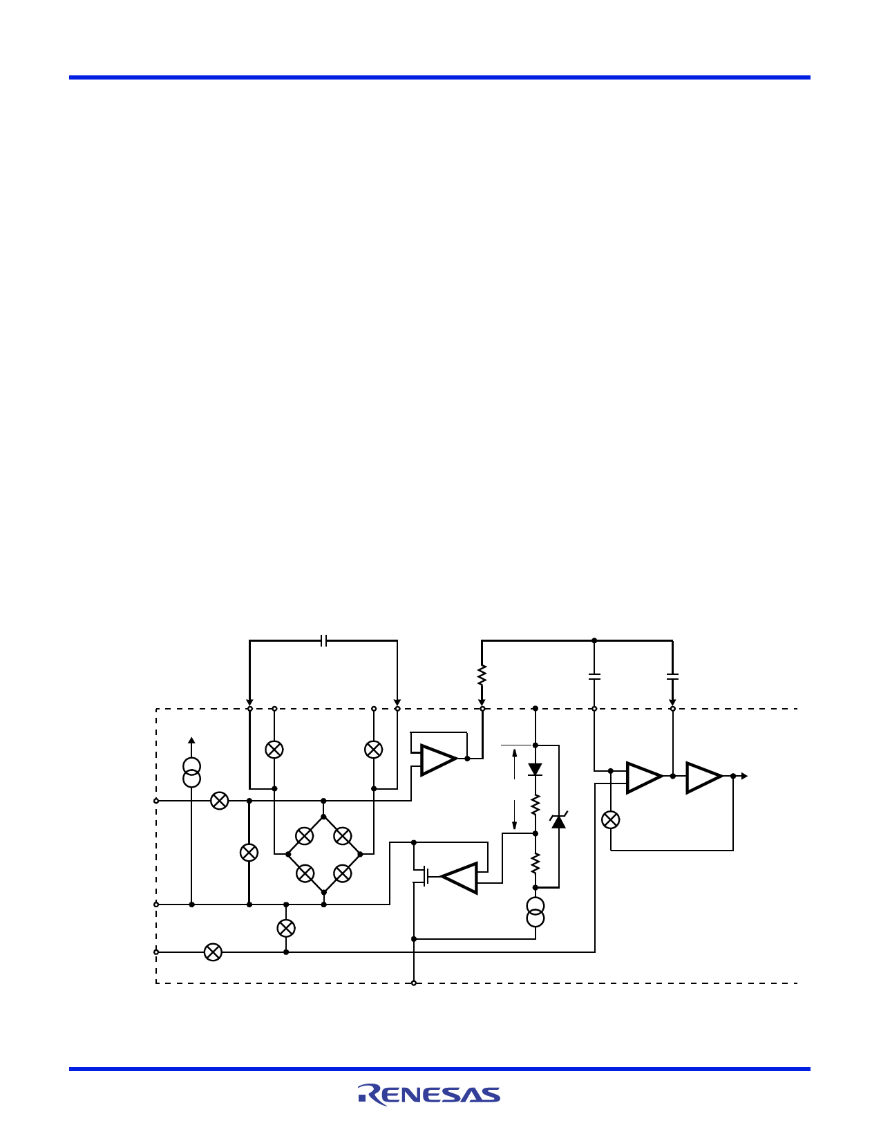
Figure 4 shows the Functional Diagram of the Analog Section
for the ICL7126. Each measurement cycle is divided into three
phases. They are (1) auto-zero (A-Z), (2) signal integrate (INT)
and (3) de-integrate (DE).
Auto-Zero Phase
During auto-zero three things happen. First, input high and low
are disconnected from the pins and internally shorted to analog
COMMON. Second, the reference capacitor is charged to the
reference voltage. Third, a feedback loop is closed around the
system to charge the auto-zero capacitor CAZ to compensate
for offset voltages in the buffer amplifier, integrator, and
comparator. Since the comparator is included in the loop, the
A-Z accuracy is limited only by the noise of the system. In any
case, the offset referred to the input is less than 10V.
Signal Integrate Phase
During signal integrate, the auto-zero loop is opened, the
internal short is removed, and the internal input high and low
are connected to the external pins. The converter then
integrates the differential voltage between IN HI and IN LO for
a fixed time. This differential voltage can be within a wide
common mode range: up to 1V from either supply. If, on the
other hand, the input signal has no return with respect to the
converter power supply, IN LO can be tied to analog COMMON
to establish the correct common mode voltage. At the end of
this phase, the polarity of the integrated signal is determined.
De-integrate Phase
The final phase is de-integrate, or reference integrate. Input
low is internally connected to analog COMMON and input high
is connected across the previously charged reference
capacitor. Circuitry within the chip ensures that the capacitor
will be connected with the correct polarity to cause the
integrator to output to return to zero. The time required for the
output to return to zero is proportional to the input signal.
Specifically, the digital reading displayed is:
Display
Count
=
1000
V---V-R---I-E-N---F--
.
Differential Input
The input can accept differential voltages anywhere within the
common mode range of the input amplifier, or specifically from
0.5V below the positive supply to 1V above the negative
supply. In this range, the system has a CMRR of 86dB typical.
However, care must be exercised to assure the integrator
output does not saturate. A worst case condition would be a
large positive common mode voltage with a near full-scale
negative differential input voltage. The negative input signal
drives the integrator positive when most of its swing has been
used up by the positive common mode voltage. For these
critical applications the integrator output swing can be reduced
to less than the recommended 2V full scale swing with little
loss of accuracy. The integrator output can swing to within 0.5V
of either supply without loss of linearity.
CREF
CREF+ REF HI
V+
34
36
REF LO CREF-
35
33
RINT
BUFFER V+
28
1
CAZ
A-Z
29
CINT
INT
27
31
IN HI
1A
INT
A-Z
A-Z
DE-
DE+
-
+
INPUT
HIGH
2.8V
INTEGRATOR
-
+
+
6.2V
A-Z
A-Z
32
COMMON
30
IN LO
INT
N
DE+
DE-
+
-
A-Z AND DE
26
V-
COMPARATOR
INPUT
LOW
FIGURE 4. ANALOG SECTION OF ICL7126
TO
DIGITAL
SECTION
FN3084 Rev.5.00
Oct 25, 2004
Page 6 of 15
Share Link: 