ICL7126 View Datasheet(PDF) - Renesas Electronics
Part Name
Description
Manufacturer
ICL7126 Datasheet PDF : 15 Pages
| |||
ICL7216
V+
ICL7126
BP 21
TEST
37
1M
TO LCD
DECIMAL
POINT
TO LCD
BACKPLANE
V+
V+
BP
ICL7126
DECIMAL
POINT
SELECT
TO LCD
DECIMAL
POINTS
TEST
V+ = DP ON
GND = DP OFF
CD4030
GND
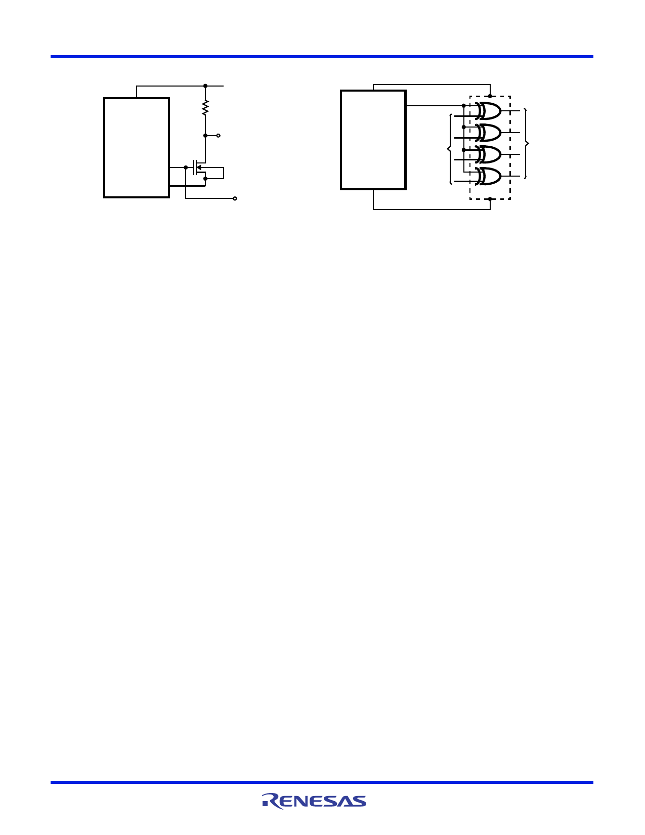
FIGURE 7. EXCLUSIVE ‘OR’ GATE FOR
DECIMAL POINT DRIVE
TEST
The TEST pin serves two functions. It is coupled to the
internally generated digital supply through a 500 resistor.
Thus it can be used as the negative supply for externally
generated segment drivers such as decimal points or any other
presentation the user may want to include on the LCD display.
Figures 6 and 7 show such an application. No more than a
1mA load should be applied.
The second function is a “lamp test”. When TEST is pulled high
(to V+) all segments will be turned on and the display should
read “-1888”. The TEST pin will sink about 10mA under these
conditions.
CAUTION: In the lamp test mode, the segments have a constant DC voltage
(no square-wave) and may burn the LCD display if left in this mode for several
minutes.
Digital Section
Figure 8 shows the digital section for the ICL7126. An internal
digital ground is generated from a 6V Zener diode and a large
P-Channel source follower. This supply is made stiff to absorb the
relative large capacitive currents when the back plane (BP)
voltage is switched. The BP frequency is the clock frequency
divided by 800. For three readings/second this is a 60Hz square
wave with a nominal amplitude of 5V. The segments are driven at
the same frequency and amplitude and are in phase with BP
when OFF, but out of phase when ON. In all cases negligible DC
voltage exists across the segments. The polarity indication is “ON”
for negative analog inputs. If IN LO and IN HI are reversed, this
indication can be reversed also, if desired.
System Timing
Figure 9 shows the clocking arrangement used in the ICL7126.
Two basic clocking arrangements can be used:
Figure 9A, an external oscillator connected to pin 40.
Figure 9B, an R-C oscillator using all three pins.
The oscillator frequency is divided by four before it clocks the
decade counters. It is then further divided to form the three
convert-cycle phases. These are signal integrate (1000 counts),
reference de-integrate (0 to 2000 counts) and auto-zero (1000 to
3000 counts). For signals less than full-scale, auto-zero gets the
unused portion of reference de-integrate. This makes a complete
measure cycle of 4,000 counts (16,000 clock pulses) independent
of input voltage. For three readings/second, an oscillator
frequency of 48kHz would be used.
To achieve maximum rejection of 60Hz pickup, the signal
integrate cycle should be a multiple of 60Hz. Oscillator
frequencies of 60kHz, 48kHz, 40kHz, 331/3kHz, etc. should
be selected. For 50Hz rejection, oscillator frequencies of
662/3kHz, 50kHz, 40kHz, etc. would be suitable. Note that
40kHz (2.5 readings/sec.) will reject both 50Hz and 60Hz
(also 400Hz and 440Hz).
FN3084 Rev.5.00
Oct 25, 2004
Page 8 of 15
Share Link: 