650R-27ILF View Datasheet(PDF) - Integrated Device Technology
Part Name
Description
Manufacturer
650R-27ILF Datasheet PDF : 7 Pages
| |||
ICS650-27
NETWORKING CLOCK SOURCE
CLOCK SYNTHESIZER
External Components
The ICS650-27 requires a minimum number of external
components for proper operation.
Decoupling Capacitor
Decoupling capacitors of 0.01µF must be connected
between each VDD and GND (pins 4 and 6, pins 16 and 14),
as close to the device as possible. For optimum device
performance, the decoupling capacitor should be mounted
on the component side of the PCB. Avoid the use of vias in
the decoupling circuit.
Series Termination Resistor
When the PCB trace between the clock outputs and the
loads are over 1 inch, series termination should be used. To
series terminate a 50Ω trace (a commonly used trace
impedance), place a 33Ωresistor in series with the clock line
as close to the clock output pin as possible. The nominal
impedance of the clock output is 20Ω.
Crystal Information
The crystal used should be a fundamental mode (do not use
third overtone), parallel resonant. Crystal capacitors should
be connected from pins X1 to ground and X2 to ground to
optimize the initial accuracy. The value of these capacitors
is given by the following equation:
Crystal caps (pF) = (CL - 6) x 2
In the equation, CL is the crystal load capacitance. So, for a
crystal with a 16pF load capacitance, two 20 pF [(16-6) x 2]
capacitors should be used.
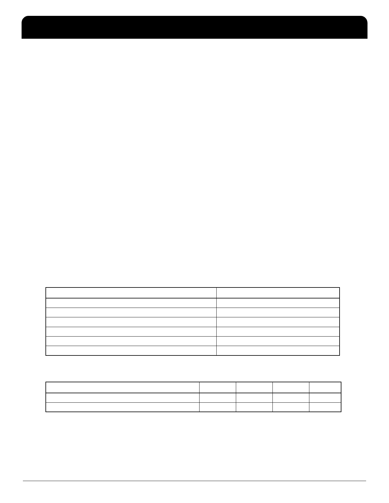
Absolute Maximum Ratings
Stresses above the ratings listed below can cause permanent damage to the ICS650-27. These ratings, which are
standard values for IDT commercially rated parts, are stress ratings only. Functional operation of the device at these
or any other conditions above those indicated in the operational sections of the specifications is not implied.
Exposure to absolute maximum rating conditions for extended periods can affect product reliability. Electrical
parameters are guaranteed only over the recommended operating temperature range.
Item
Supply Voltage, VDD
All Inputs and Outputs
Ambient Operating Temperature
Storage Temperature
Junction Temperature
Soldering Temperature
Rating
7V
-0.5 V to VDD+0.5 V
-40 to +85° C
-65 to +150° C
175° C
260° C
Recommended Operation Conditions
Parameter
Ambient Operating Temperature
Power Supply Voltage (measured in respect to GND)
Min.
-40
+3.0
Typ.
+3.3
Max.
+85
+3.6
Units
°C
V
IDT™ / ICS™ NETWORKING CLOCK SOURCE
4
ICS650-27 REV F 051310
Share Link: 