SC28C198A1A View Datasheet(PDF) - Philips Electronics
Part Name
Description
Manufacturer
SC28C198A1A Datasheet PDF : 56 Pages
| |||
Philips Semiconductors
Octal UART for 3.3V and 5V supply voltage
Product specification
SC28L198
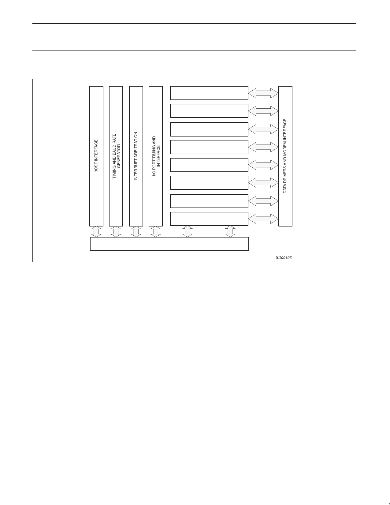
BLOCK DIAGRAM
FULL DUPLEX UART CHANNEL
FULL DUPLEX UART CHANNEL
FULL DUPLEX UART CHANNEL
FULL DUPLEX UART CHANNEL
FULL DUPLEX UART CHANNEL
FULL DUPLEX UART CHANNEL
FULL DUPLEX UART CHANNEL
FULL DUPLEX UART CHANNEL
INPUT BUFFERS AND OUTPUT DRIVERS
Block Diagram SC28C/28L198
SD00193
As shown in the block diagram, the Octal UART consists of: an
interrupt arbiter, host interface, timing blocks and eight UART
channel blocks. The eight channels blocks operate independently,
interacting only with the timing, host I/F and interrupt blocks.
FUNCTIONAL DESCRIPTION
The SC28L198 is composed of several functional blocks:
• Synchronous host interface block
• A timing block consisting of a common baud rate generator
making 22 industry standard baud rates and 2 16–bit counters
used for non–standard baud rate generation
• 4 identical independent full duplex UART channel blocks
• Interrupt arbitration system evaluating 24 contenders
• I/O port control section and change of state detectors.
occurs in the C4 time and occurs approximately 18 ns after the
rising edge of C4.
Addressing of the various functions of the OCTART is through the
address bus A(7:0). The 28L198 is compatible with the SC28L198
OCTAL UART in software and function. A[7], in a general sense, is
used to separate the data portion of the circuit from the control
portion.
Asynchronous bus cycle
The asynchronous mode requires one bus cycle of the chip select
(CEN) for each read or write to the chip. No more action will occur
on the bus after the C4 time until CEN is returned high.
Synchronous bus cycle
In the synchronous mode a read or write will be done every four
cycles of the Sclk. CEN does not require cycling but must remain
low to keep the synchronous accesses active. This provides a burst
mode of access to the chip.
CONCEPTUAL OVERVIEW
Host Interface
The Host interface is comprised of the signal pins CEN, W/RN,
IACKN, DACKN, IRQN Sclk and provides all the control for data
transfer between the external and internal data buses of the host
and the OCTART. The host interface operates in a synchronous
mode with the system (Sclk) which has been designed for a nominal
operating frequency of 33 MHz. The interface operates in either of
two modes; synchronous or asynchronous to the Sclk However
the bus cycle within the OCTART always takes place in four Sclk
cycles after CEN is recognized. These four cycles are the C1, C2,
C3, C4 periods shown in the timing diagrams. DACKN always
In both cases each read or write operation(s) will be completed in
four (4) Sclk cycles. The difference in the two modes is only that the
asynchronous mode will not begin another bus cycle if the CEN
remains active after the four internal Sclk have completed. Internally
the asynchronous cycle will terminate after the four periods of Sclk
regardless of how long CEN is held active
In all cases the internal action will terminate at the withdrawal of
CEN. Synchronous CEN cycles shorter than multiples of four Sclk
cycles minus 1 Sclk and asynchronous CEN cycles shorter than four
Sclk cycles may cause short read or write cycles and produce
corrupted data transfers.
Timing Circuits
The timing block consists of a crystal oscillator, a fixed baud rate
generator (BRG), a pair of programmable 16 bit register based
1999 Jan 14
7
Share Link: 