MC141531 View Datasheet(PDF) - Motorola => Freescale
Part Name
Description
Manufacturer
MC141531 Datasheet PDF : 25 Pages
| |||
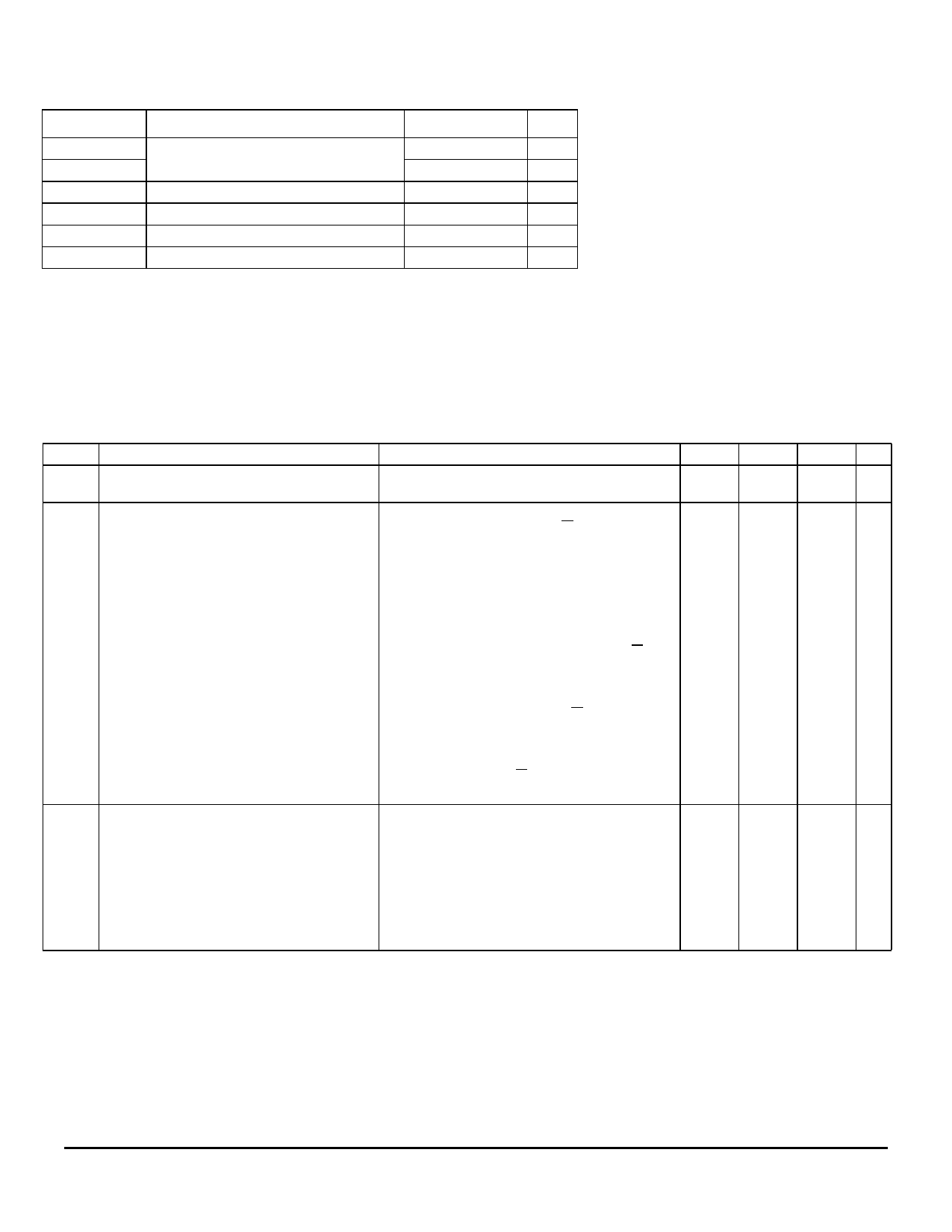
MAXIMUM RATINGS* (Voltages Referenced to VSS, TA=25˚C)
Symbol
Parameter
Value
Unit
AVDD,DVDD
VCC
Vin
I
TA
Tstg
Supply Voltage
-0.3 to +4.0
V
VSS-0.3 to VSS+10.5 V
Input Voltage
VSS-0.3 to VDD+0.3 V
Current Drain Per Pin Excluding VDD and VSS
25
mA
Operating Temperature
-30 to +85
˚C
Storage Temperature Range
-65 to +150
˚C
* Maximum Ratings are those values beyond which damage to the device may occur. Functional
operation should be restricted to the limits in the Electrical Characteristics tables or Pin Descrip-
tion section.
VSS = AVSS = DVSS (DVSS = VSS of Digital circuit, AVSS = VSS of Analogue Circuit)
VDD = AVDD = DVDD (DVDD = VDD of Digital circuit, AVDD = VDD of Analogue Circuit)
This device contains circuitry to protect the inputs
against damage due to high static voltages or elec-
tric fields; however, it is advised that normal precau-
tions to be taken to avoid application of any voltage
higher than maximum rated voltages to this high
impedance circuit. For proper operation it is recom-
mended that Vin and Vout be constrained to the
range VSS < or = (Vin or Vout) < or = VDD. Reliability
of operation is enhanced if unused input are con-
nected to an appropriate logic voltage level (e.g.,
either VSS or VDD). Unused outputs must be left
open. This device may be light sensitive. Caution
should be taken to avoid exposure of this device to
any light source during normal operation. This
device is not radiation protected.
ELECTRICAL CHARACTERISTICS (Voltage Referenced to VSS, VDD=2.4 to 3.5V, TA=25˚C)
Symbol
Parameter
Test Condition
Min
Typ
Max Unit
DVDD Logic Circuit Supply Voltage Range
(Absolute value referenced to VSS)
AVDD DC/DC Converter Circuit Supply Voltage Range
2.4
3.0
3.5
V
2.4
-
3.5
V
IAC Access Mode Supply Current Drain
(AVDD + DVDD Pins)
IDP Display Mode Supply Current Drain
(AVDD + DVDD Pins)
VDD=3.0V, Internal DC/DC Converter On, Tripler
0
Enabled, Annunciator On/Off, R/W accessing,
Tcyc=1MHz, Osc. Freq.=38.4kHz, Display On, 1/7
Mux Ratio
VDD=3.0V, Internal DC/DC Converter On, Tripler
0
Enabled,
Annunciator On/Off, R/W halt, Osc. Freq.=38.4kHz,
200
300 µA
75
165 µA
ISB1 Standby Mode Supply Current Drain
(AVDD + DVDD Pins)
Display On, 1/17Mux Ratio
0
VDD=3.0V, Display off, Oscillator Disabled, R/W halt.
300
500 nA
ISB2 Annunciator Mode Supply Current Drain
(AVDD + DVDD Pins)
ISB3 Icon Mode Supply Current Drain
(AVDD + DVDD Pins)
VCC1 LCD Driving DC/DC Converter Output
(VCC Pin)
VDD=3.0V, Annunciator Mode, Internal Oscillator,
Oscillator Enabled, Display Off, R/W halt, Int Osc.
Freq.=38.4kHz.
VDD=3.0V, Icon Mode, Internal Oscillator, Oscillator
Enabled, Display Off, R/W halt, Ext Osc.
Freq.=38.4kHz.
Display On, Internal DC/DC Converter Enabled,
Tripler Enabled, Osc. Freq.=38.4KHz,
Regulator Enabled, Divider Enabled.
0
5
10
µA
0
-
25
µA
-
3*AVDD 10.5
V
VCC2 LCD Driving DC/DC Converter Output
(VCC Pin)
Display On, Internal DC/DC Converter Enabled,
Doubler Enabled, Osc. Freq.=38.4KHz,
Regulator Enabled, Divider Enabled.
-
2*AVDD
7
V
VLCD LCD Driving Voltage Input (VCC Pin)
Internal DC/DC Converter Disabled.
5
-
10.5 V
MOTOROLA
MC141531
3–143
Share Link: 