TS4962 View Datasheet(PDF) - STMicroelectronics
Part Name
Description
Manufacturer
TS4962 Datasheet PDF : 22 Pages
| |||
TS4962
Absolute Maximum Ratings
1 Absolute Maximum Ratings
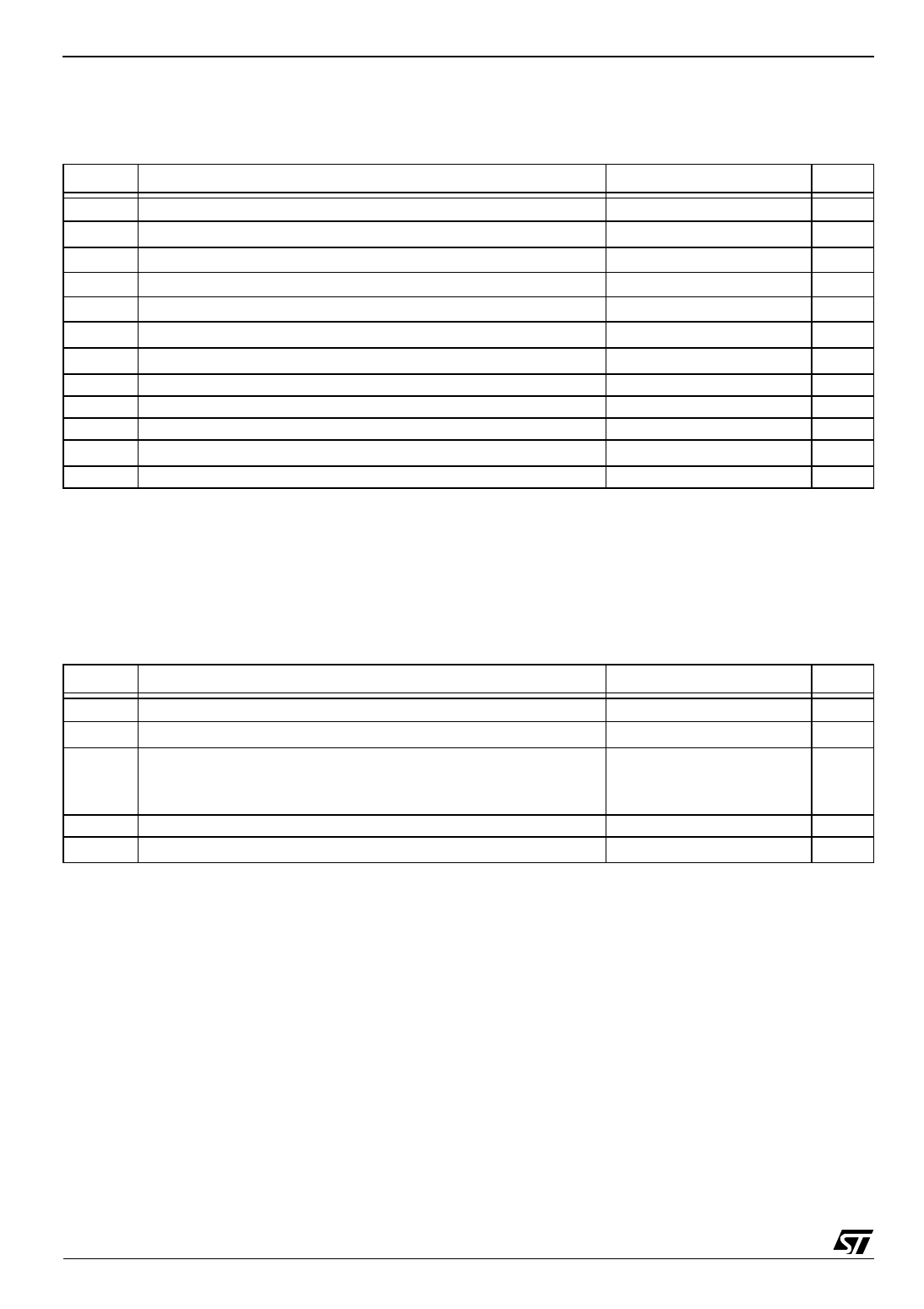
Table 1. Key parameters and their absolute maximum ratings
Symbol
Parameter
Value
VCC Supply voltage 1
Vi
Toper
Tstg
Tj
Rthja
Pd
Input Voltage 2
Operating Free Air Temperature Range
Storage Temperature
Maximum Junction Temperature
Thermal Resistance Junction to Ambient 3
Power Dissipation
ESD Human Body Model
ESD Machine Model
Latch-up Latch-up Immunity
VSTB Standby pin voltage maximum voltage 5
Lead Temperature (soldering, 10sec)
6
GND to VCC
-40 to + 85
-65 to +150
150
200
Internally Limited4
2
200
200
GND to VCC
260
1) All voltages values are measured with respect to the ground pin.
2) The magnitude of input signal must never exceed VCC + 0.3V / GND - 0.3V
3) Device is protected in case of over temperature by a thermal shutdown active @ 150°C.
4) Exceeding the power derating curves during a long period, involves abnormal operating condition.
5) The magnitude of standby signal must never exceed VCC + 0.3V / GND - 0.3V
Table 2. Operating Conditions
Symbol
Parameter
VCC
VIC
VSTB
Supply Voltage1
Common Mode Input Voltage Range2
Standby Voltage Input : 3
Device ON
Device OFF
RL
Rthja
Load Resistor
Thermal Resistance Junction to Ambient 5
1) For VCC from 2.4V to 2.5V, the operating temperature range is reduced to 0°C≤ Tamb ≤70°C
2) For VCC from 2.4V to 2.5V, the common mode input range must be set at VCC/2.
3) Without any signal on VSTB, the device will be in standby
4) Minimum current consumption shall be obtained when VSTB = GND.
5) With heat sink surface = 125mm2.
Value
2.4 to 5.5
0.5 to VCC-0.8
1.4 ≤ VSTB ≤ VCC
GND ≤ VSTB ≤ 0.4 4
≥4
90
Unit
V
V
°C
°C
°C
°C/W
kV
V
mA
V
°C
Unit
V
V
V
Ω
°C/W
2/22
Share Link: 