MSM9810B View Datasheet(PDF) - Oki Electric Industry
Part Name
Description
Manufacturer
MSM9810B Datasheet PDF : 45 Pages
| |||
OKI Semiconductor
FEDL9810BFULL-03
MSM9810B
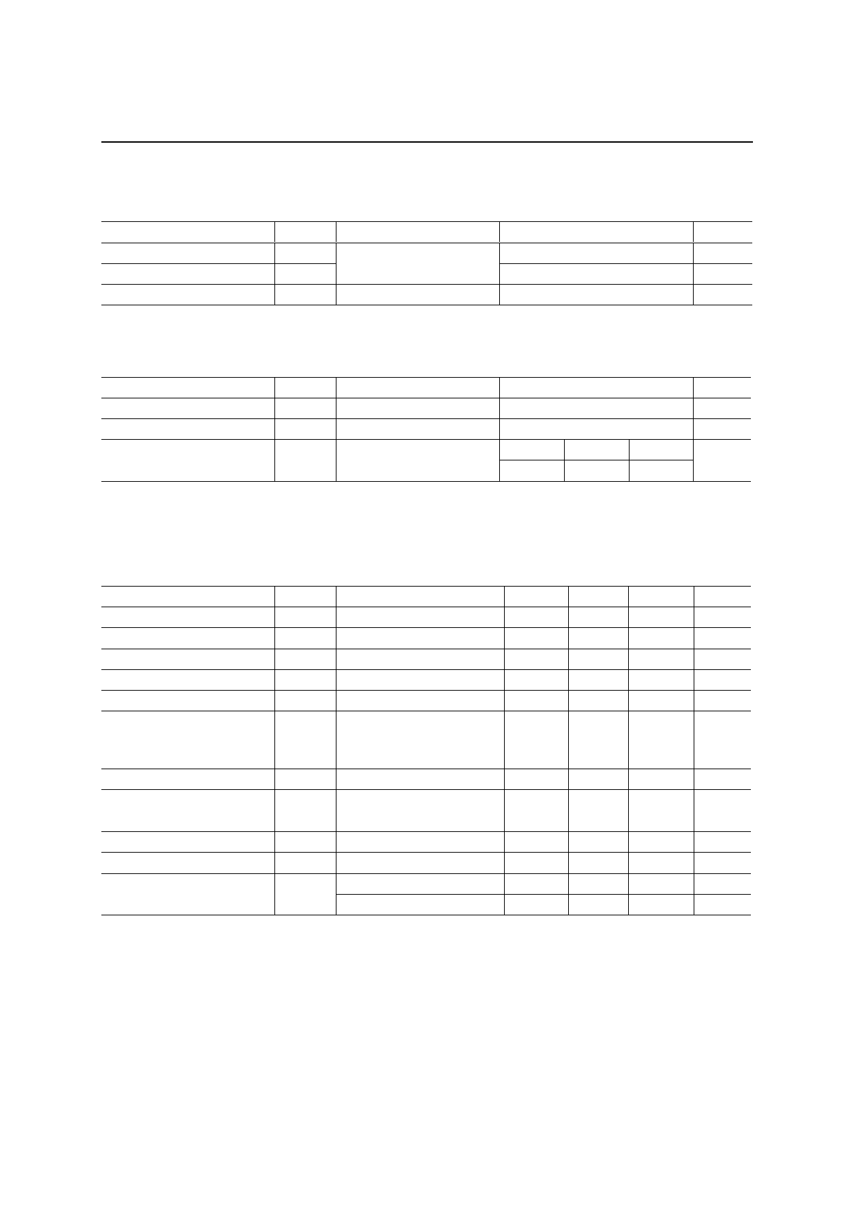
ABSOLUTE MAXIMUM RATINGS
Parameter
Power Supply Voltage
Input Voltage
Storage Temperature
Symbol
VDD
VIN
TSTG
Condition
Ta= 25°C
—
Rating
–0.3 to +7.0
–0.3 to VDD+ 0.3
–55 to +150
(GND = 0 V)
Unit
V
V
°C
RECOMMENDED OPERATING CONDITIONS
Parameter
Power Supply Voltage
Operating Temperature
Master Clock Frequency
Symbol
VDD
Top
fOSC
Condition
—
—
—
(GND = 0 V)
Range
Unit
4.5 to 5.5
V
–40 to +85
°C
Min.
Typ.
Max.
MHz
3.5
4.096
4.5
ELECTRICAL CHARACTERISTICS
DC Characteristics
Parameter
High-level Input Voltage
Low-level Input Voltage
High-level Output Voltage
Low-level Output Voltage
High-level Input Current 1
Symbol
VIH
VIL
VOH
VOL
IIH1
(DVDD = AVDD = 4.5 to 5.5 V, DGND = AGND = 0 V, Ta = –40 to +85°C)
Condition
Min.
Typ.
Max.
Unit
—
0.84 × VDD —
—
V
—
—
— 0.16 × VDD V
IOH = –1 mA
VDD – 0.4 —
—
V
IOL = 2 mA
—
—
0.4
V
VIH = VDD
—
—
10
µA
High-level Input Current 2
Applied to pins with internal
(Note 1)
IIH2
pull-down resistor
30
—
300
µA
Low-level Input Current 1
IIL1
VIL = GND
–10
—
Low-level Input Current 2
Applied to pins with internal
(Note 2)
IIL2
pull-up resistor
–300
—
Output Leakage Current
ILO
0 ≤ VOUT ≤ VDD
–10
—
Operating Current
Standby Current
IDD
fOSC 4 MHz, no load
Ta = –40 to +70°C
IDS
Ta = +70 to +85°C
—
6
—
—
—
—
—
µA
–30
µA
+10
µA
15
mA
15
µA
50
µA
Notes 1: Applicable to RD7 to RD0 pins (when RCS = “H”).
2: Applicable to CMD, RD, WR, and CS pins.
6/45
Share Link: 