AS6C3216A-55BIN View Datasheet(PDF) - Alliance Semiconductor
Part Name
Description
Manufacturer
AS6C3216A-55BIN Datasheet PDF : 11 Pages
| |||
AS6C3216A-55BIN
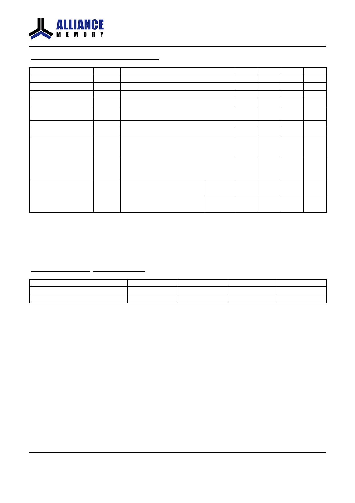
DC ELECTRICAL CHARACTERISTICS
PARAMETER SYMBOL
TEST CONDITION
Supply Voltage
Input High Voltage
Input Low Voltage
VCC
VIH*1
VIL*2
Input Leakage Current
ILI
VCC ≧VIN ≧VSS
Output Leakage
Current
ILO
VCC ≧VOUT ≧VSS
Output Disabled
Output High Voltage
VOH IOH = -1mA
Output Low Voltage
VOL IOL = 2mA
Cycle time = MIN.
Average Operating
Power supply Current
ICC CE#≦0.2V and CE2≧VCC-0.2V,II/O = 0mA
Other pins at 0.2V or VCC-0.2V
Cycle time = 1µs
ICC1 CE#≦0.2V and CE2≧VCC-0.2V,II/O = 0mA
Other pins at 0.2V or VCC-0.2V
Standby Power
Supply Current
ISB1
CE#≧VCC-0.2V or CE2≦0.2V
Other pins at 0.2V or VCC-0.2V
40℃
85℃
MIN.
2.7
2.2
- 0.2
-1
-1
2.2
-
-
-
-
-
TYP. *4 MAX.
3.0
3.6
- VCC+0.3
-
0.6
-
1
UNIT
V
V
V
µA
-
1
µA
2.7
-
V
-
0.4
V
12
20
mA
3
5
mA
8
18
µA
-
80
µA
Notes:
1. VIH(max) = VCC + 2.0V for pulse width less than 6ns.
2. VIL(min) = VSS - 2.0V for pulse width less than 6ns.
3. Over/Undershoot specifications are characterized on engineering evaluation stage, not for mass production test.
4. Typical values, measured at VCC = VCC(TYP.) and TA = 25℃, are included for reference only and are not guaranteed or tested.
CAPACITANCE (TA = 25℃, f = 1.0MHz)
PARAMETER
SYMBOL
MIN.
Input Capacitance
CIN
-
Input/Output Capacitance
CI/O
-
Note : These parameters are guaranteed by device characterization, but not production tested.
MAX.
8
8
UNIT
pF
pF
Confidential
- 4 of 11 -
Rev.1.0 June 2017
Share Link: 