STK672-543-E View Datasheet(PDF) - ON Semiconductor
Part Name
Description
Manufacturer
STK672-543-E Datasheet PDF : 22 Pages
| |||
STK672-543-E
Specifications
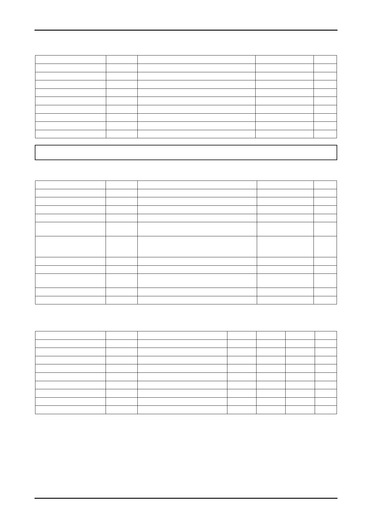
Absolute Maximum Ratings at Tc = 25°C
Parameter
Maximum supply voltage 1
Maximum supply voltage 2
Input voltage
Output current 1
Output current 2
Allowable power dissipation
Operating substrate temperature
Junction temperature
Storage temperature
Symbol
VCC max
VDD max
VIN max
IOP max
IOH max
Pd max
Tc max
Tj max
Tstg
Conditions
No signal
No signal
Logic input pins
10μA 1 pulse (resistance load)
VDD=5V, CLOCK≥200Hz
With an arbitrarily large heat sink. Per MOSFET
Ratings
unit
52
V
-0.3 to +7.0
V
-0.3 to +7.0
V
10
A
4
A
13.3
W
105
°C
150
°C
-40 to +125
°C
Stresses exceeding Maximum Ratings may damage the device. Maximum Ratings are stress ratings only. Functional operation above the Recommended Operating
Conditions is not implied. Extended exposure to stresses above the Recommended Operating Conditions may affect device reliability.
Allowable Operating Ranges at Ta=25°C
Parameter
Symbol
Conditions
Ratings
unit
Operating supply voltage 1
VCC
With signals applied
10 to 42
V
Operating supply voltage 2
VDD
With signals applied
5±5%
V
Input high voltage
Input low voltage
VIH
Pins 8, 9, 10, 11, 12
VIL
Pins 8, 9, 10, 11, 12
2.5 to VDD
V
0 to 0.6
V
Output current 1
IOH1
Tc=105°C, CLOCK≥200Hz,
Continuous operation, duty=100%
3.0
A
Output current 2
IOH2
Tc=80°C, CLOCK≥200Hz,
Continuous operation, duty=100%,
3.3
A
CLOCK frequency
See the motor current (IOH) derating curve
fCL
Minimum pulse width: at least 10μs
0 to 50
kHz
Phase driver withstand voltage
VDSS
ID=1mA (Tc=25°C)
100min
V
Recommended operating
Tc
substrate temperature
No condensation
0 to 105
°C
Recommended Vref range
Vref
Tc=105°C
0.14 to 1.62
V
Input rise and fall slew rate
tr/tf
2.6max
V
Refer to the graph for each conduction-period tolerance range for the output current and brake current.
Electrical Characteristics at Tc=25°C, VCC=24V, VDD=5.0V
Parameter
Symbol
Conditions
VDD supply current
Output average current
ICCO
Ioave
Pin 6 current CLOCK=GND
R/L=3Ω/3.8mH in each phase
FET diode forward voltage
Output saturation voltage
Input high voltage
Input low voltage
Input leak current
Vref input bias current
PWM frequency
Vdf
Vsat
VIH
VIL
IIL
IIB
fc
If=1A (RL=23Ω)
RL=23Ω
Pins 8, 9, 10, 11, 12
Pins 8, 9, 10, 11, 12
Pins 8, 9, 10, 11, 12=GND and 5V
Pin 7 =1.0V
Notes: A fixed-voltage power supply must be used.
min
0.52
2.5
35
typ
3.1
0.58
1.0
0.28
204
45
max
unit
7
mA
0.64
A
1.6
V
0.40
V
V
0.6
V
±10
μA
216
μA
55 kHz
No. A2113-2/22
Share Link: 