SMC032BF View Datasheet(PDF) - STMicroelectronics
Part Name
Description
Manufacturer
SMC032BF Datasheet PDF : 91 Pages
| |||
SMCxxxBF
Electrical interface
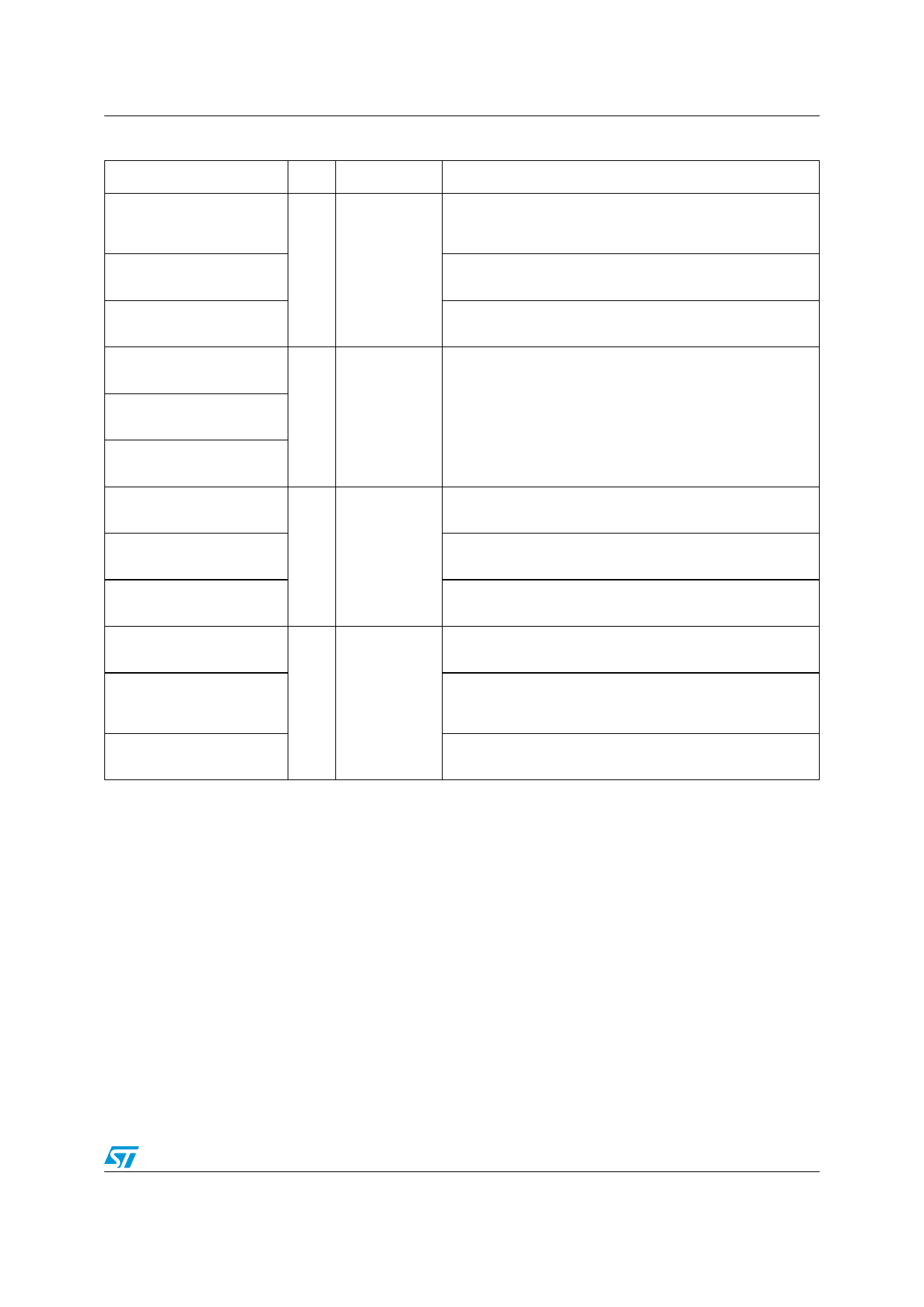
Table 9. Signal Description (continued)
Signal Name
Dir.
Pin
–VS1, –VS2
(PC Card Memory Mode)
–VS1, –VS2
O
(PC Card I/O Mode)
–VS1, –VS2
(True IDE Mode)
–WAIT
(PC Card Memory Mode)
–WAIT
O
(PC Card I/O Mode)
IORDY
(True IDE Mode)
–WE
(PC Card Memory Mode)
–WE
I
(PC Card I/O Mode)
–WE
(True IDE Mode)
WP
(PC Card Memory Mode)
33,40
42
36
–IOIS16
(PC Card I/O Mode)
O
24
–IOCS16
(True IDE Mode)
Description
Voltage Sense Signals.–VS1 is grounded so that the CIS
can be read at 3.3 volts and –VS2 is reserved by PCMCIA
for a secondary voltage.
Same for all modes.
Same for all modes.
ST CF does not assert the WAIT (IORDY) signal
Driven by the host to strobe memory write data to the
registers.
Used for writing to the configuration registers.
Not used, should be connected to VCC by the host.
No write protect switch available. It is held Low after the
completion of the reset initialization sequence.
Used for the 16 bit Port (–IOIS16) function. Low indicates
that a 16 bit or odd Byte only operation can be performed at
the addressed port.
Asserted Low when the Card is expecting a Word data
transfer cycle.
21/91
Share Link: 