ZL60102MJD View Datasheet(PDF) - Zarlink Semiconductor Inc
Part Name
Description
Manufacturer
ZL60102MJD Datasheet PDF : 20 Pages
| |||
ZL60101/2
Data Sheet
Absolute Maximum Ratings
Not necessarily applied together. Exceeding these values may cause permanent damage. Functional operation
under these conditions is not implied.
Parameter
Symbol
Supply voltage
VCC
Differential input voltage amplitude1
∆V
Voltage on any pin
Relative humidity (non-condensing)
Storage temperature
ESD resistance
1. Differential input voltage amplitude is defined as ∆V = DIN+ − DIN-.
VPIN
MOS
TSTG
VESD
Recommended Operating Conditions
These parameters apply both to the transmitter and the receiver.
Min.
Max.
Unit
-0.3
4.0
V
1.2
V
-0.3
VCC + 0.3
V
5
95
%
-40
100
°C
±1
kV
Parameter
Symbol
Min.
Max.
Unit
Power supply voltage
VCC
3.135
3.465
V
Operating case temperature
Signaling rate (per channel)1
Link distance2
TCASE
0
fD
1.0
LD
2
80
°C
2.72
Gbps
m
Data I/O DC blocking capacitors3
Power supply noise4
CBLK
100
VNPS
nF
200
mVp-p
1. Data patterns are to have maximum run lengths and DC balance shifts no worse than that of a Pseudo Random Bit Sequence of
length 223-1 (PRBS-23). Information on lower bit rates is available on request.
2. For maximum distance, see Table 6.
3. For AC-coupling, DC blocking capacitors external to the module with a minimum value of 100 nF is recommended.
4. Power supply noise is defined at the supply side of the recommended filter for all VCC supplies over the frequency range of 500 Hz
to 2720 MHz with the recommended power supply filter in place.
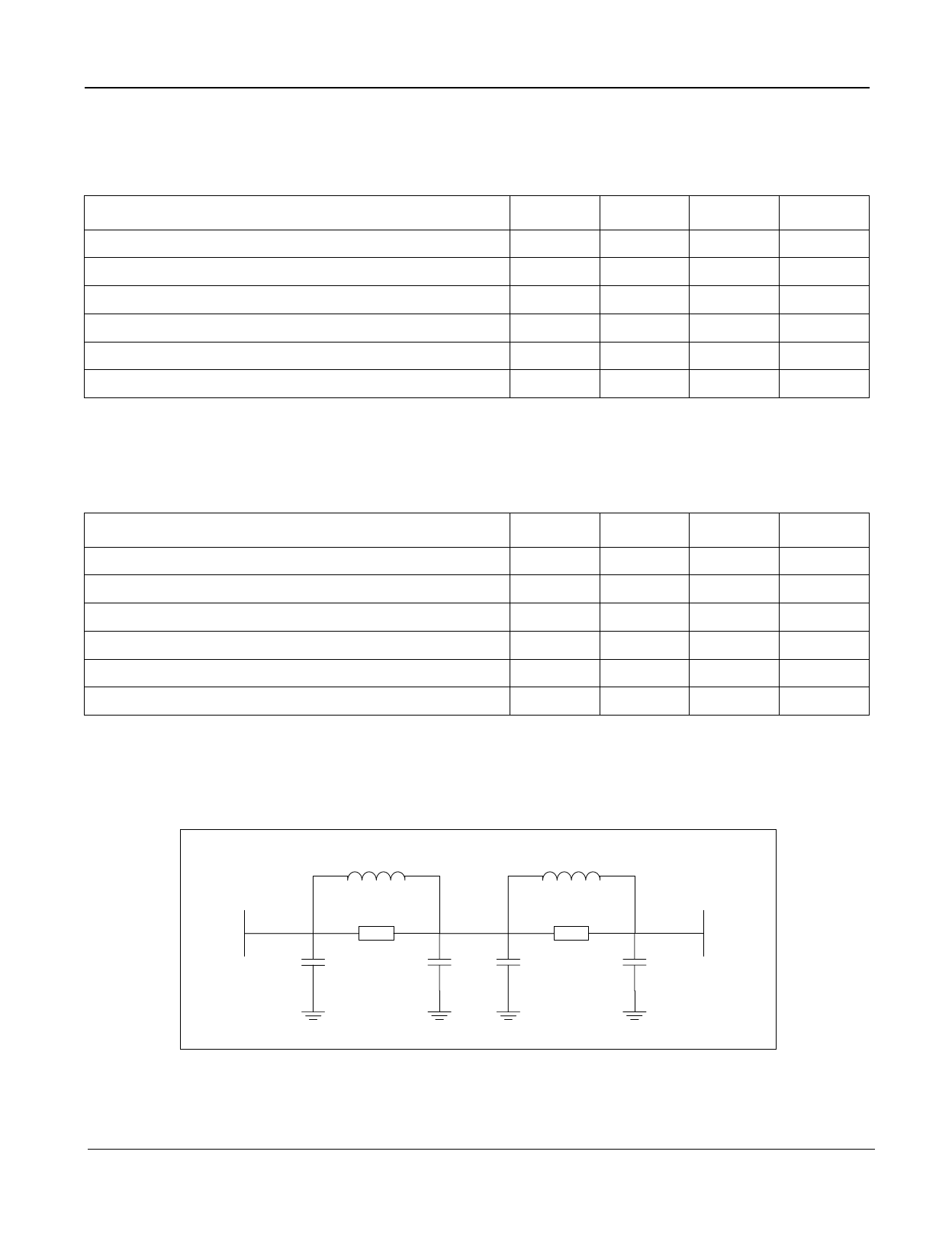
L1 1 µH
L2 6.8 nH
Host
Vcc
C1
10 µF
R1 100 Ω
C2
10 µF
R2 1.0 kΩ
C3
0.1 µF
C4
0.1 µF
Module
Vcc
Figure 1 - Recommended Power Supply Filter
3
Zarlink Semiconductor Inc.
Share Link: 