CPC5710N View Datasheet(PDF) - IXYS CORPORATION
Part Name
Description
Manufacturer
CPC5710N Datasheet PDF : 10 Pages
| |||
INTEGRATED CIRCUITS DIVISION
2. Using CPC5710N
2.1 LIN/CMP Input
The LIN/CMP input selects the active output, either
the detector output CMPOUT or the linear outputs,
LINOUT- and LINOUT+. Set LIN/CMP low for linear
output and high for comparator output. Note that both
outputs cannot be used at once.
With LIN/CMP at logic low (LIN/CMP = 0), the
amplifier outputs are biased at a nominal 1VDC and
CMPOUT is held high. With LIN/CMP at logic high
(LIN/CMP = 1), LINOUT+ is 0V and LINOUT- is 2V.
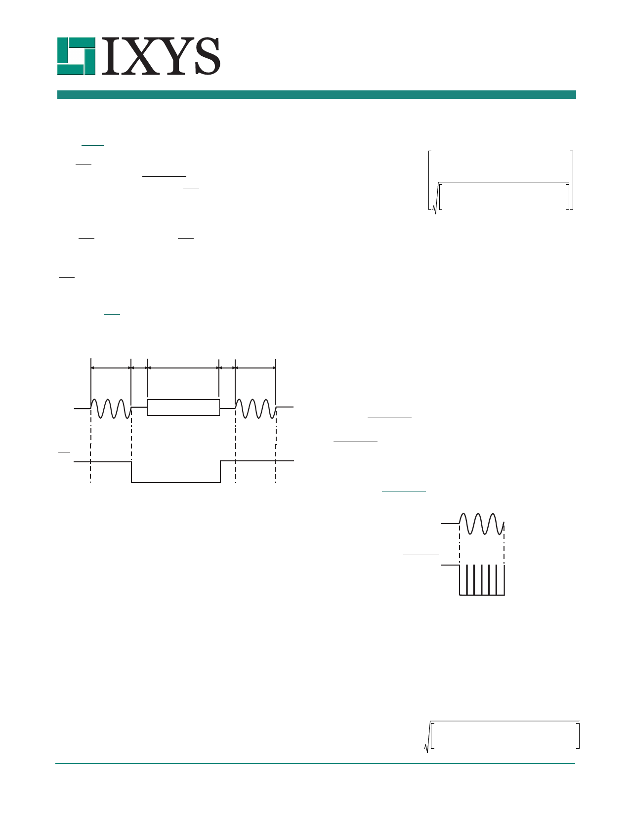
Figure 1. LIN/CMP Timing for Caller-ID Signal
Reception
2s 500 ms
3s
475 ms 2s
LIN/CMP
Caller ID data
CPC5710N
GAINCIDdB = 20log -----------------------------------6---R----S---N----P---D------------------------------------
4RSNP + RSNPD2 + -------f--C---1-S--N----P-----2-
where is the frequency of the signal.
Application Note AN-117 Customize Caller ID Gain and
Ringing Detect Voltage Threshold is a spreadsheet for
trying different component values in this type of circuit.
2.3 Detector Considerations
2.3.1 Ringing Signal Detection
The CPC5710N detector is a full-wave configuration.
Ringing signals will assert the output on both positive
and negative parts of the ringing waveform. Hysteresis
is employed by the internal comparator circuit to
provide noise immunity. The set-up of the detector
causes CMPOUT output pulses to remain low for most
of the ringing signal positive and negative half-cycles.
CMPOUT returns high when the ringing signal is near
the zero-voltage crossing.
Signal levels not to scale
2.2 Amplifier Design
Considerations
Amplifier inputs are biased at a nominal 1.25VDC, the
internal voltage reference. The internal common-mode
circuitry maintains the average of the inputs at
1.25VDC. For example, if one input reaches 1.3V, the
common-mode circuit drives the other input to 1.2V.
2.2.1 Linear Amplifier Gain
Display feature information (caller ID) and voice
signals are coupled through the linear amplifier. In
North America, CID data signals are typically sent
between the first and second ringing signal burst.
Figure 2. CMPOUT Relative to Input
Ringing Signal
CMPOUT
2.3.2 Setting Ringing Detection Threshold
The ringing detection threshold depends on the
component values of the input network. The values for
these components shown in the application circuit are
recommended for typical operation. Referring to
Figure 5., the ringing detection threshold can be
changed according to the following formula:
Referring to Figure 5., signal gain from tip and ring to
LINOUT+ and LINOUT- is determined by:
VRINGPK
=
-R-7--R-5---0S--N-m---P--V-D--
4RSNP + RSNPD2 + -------f-R----I--N---G-1---C----S---N---P------2
R03
www.ixysic.com
5
Share Link: 