LA4183 View Datasheet(PDF) - SANYO -> Panasonic
Part Name
Description
Manufacturer
LA4183 Datasheet PDF : 11 Pages
| |||
LA4183
The output of ch1 is divided with R5, R6 and led to pin 1 and then inputted to ch2. Since the attenuation degree (R5/R6) of ch1
output and the amplification degree (R4/R2 + R6)) of ch2 are fixed at an equal value, the ch2 output is in opposite phase with the
ch1 output. Therefore, the total voltage gain gets apparently 6 dB higher than the voltage gain of ch1 alone and is determined by
the following equation.
VG = 20 log R3 + 6 [dB]
R1
If the IC is used at a voltage gain less than this, the following equation with Rf added applies.
R3
VG = 20 log R1 + Rf
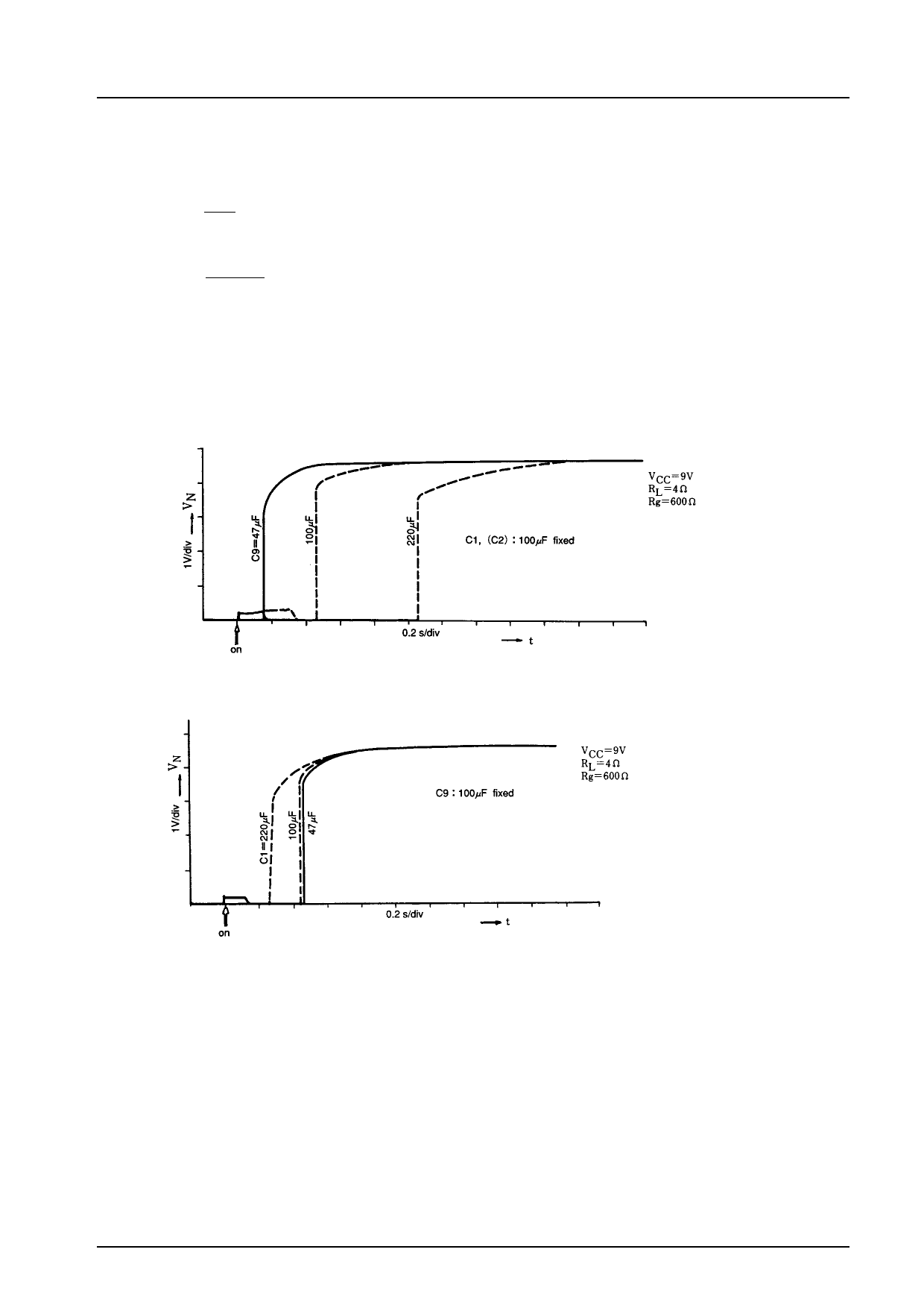
2. Starting time
+ 6 [dB]
Starting time depends on capacitance of C1 (C2) and C9 as shown in the diagram below. That is because of using a muting circuit
utilizing the C9 (decoupling capacitor) time constant for pop noise prevention when power is turned on and charging circuits for
C1 and C2 (NF capacitors).
Dependence on C9
Quiescent
Quiescent
Dependence on C1 (C2)
3. Crosstalk
Channel separation characteristic is important for single-package IC embodying two channels.
With LA4183, good channel separation is obtainable even as is, but if the BTL OUT pin (pin 1) is not grounded, it will invite
imbalance in crosstalk between the two channels. (Refer to the characteristics diagram.)
No.887-5/11
Share Link: 