LA4183 View Datasheet(PDF) - SANYO -> Panasonic
Part Name
Description
Manufacturer
LA4183 Datasheet PDF : 11 Pages
| |||
LA4183
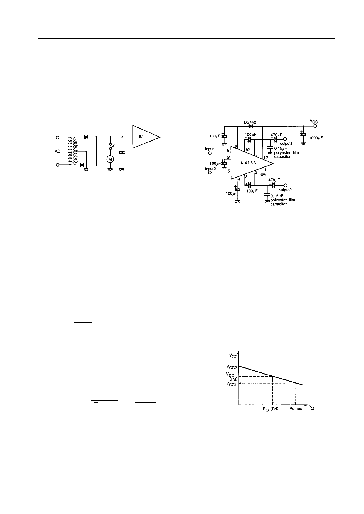
Proper Cares in Operating a Set with LA4183 Incorporated
When a set with the LA4183 incorporated is operated from AC power supply, a momentary drop in supply voltage is caused by
the transformer regulation, etc. at the time of turning ON the motor with the circuit shown below. In this case, if ripple noise is
generated from the speaker or headphone, take the following actions.
1. Connect a diode (rectifier diode of average rectified current IO = 100 to 200 mA) across pins 6 and 12 of the LA4183 so that
the voltage at pin 6 can follow the supply voltage regulation. In the steady state, this diode is cut off.
2. Increase the capacity of the power source capacitor so that the supply voltage regulation can be minimized.
Radiation Design
. Since the DIP 12-pin package is so designed as to be able to radiate heat through the Cu-foiled area of printed circuit board
under normal operating conditions, make the Cu-foiled area near the fin of IC as large as possible when designing the printed
. circuit board.
By providing the Cu-foiled area covered by the broken line as shown in the above-mentioned example of printed circuit pattern,
. a rather satisfactory radiation is enabled. (Refer to the Pd − Ta characteristics.)
Since the power dissipation (Pd) goes higher depending on the conditions of supply voltage and load, it is recommended to use
. the fin together with the printed circuit board.
The following equations are rule-of-thumb guides for Pd (for stereo). For AC power supply, it is desirable to measure with the
transformer of each individual set. In the bridge amplifier application, calculation should be made with 1/2 of the load used.
(1) DC Power supply
Pd max =
VCC2
π2RL
+ ICCO v VCC (For stereo)
(2) AC power supply
Pd max =
VCC (Pd)2
π2RL
+ ICCO v VCC (Pd) (For stereo)
VCC2: Quiescent supply voltage
ICCO: Quiescent current
VCC (Pd): Supply voltage at Pd max. output,
VCC (Pd) =
(1 + r) VCC1
√ 1 + r v VCC1 ×
√2 v π v RL
RL
PO max
VCC1: Supply voltage at max. output
r: Voltage regulation, VCC2 – VCC1
VCC1
. Example of fin mounting
The fin is formed into such a shape as to be able to radiate heat from the plastic area of IC and the fin as shown below and is
soldered to the printed circuit board. For the fin size, refer to the Pd – Ta characteristics. The desirable material is copper or
iron which is solderable. It is recommended to apply silicone grease, etc. to the plastic area of IC in order to minimize the
thermal resistance.
No.887-6/11
Share Link: 