LTC1326 View Datasheet(PDF) - Linear Technology
Part Name
Description
Manufacturer
LTC1326 Datasheet PDF : 16 Pages
| |||
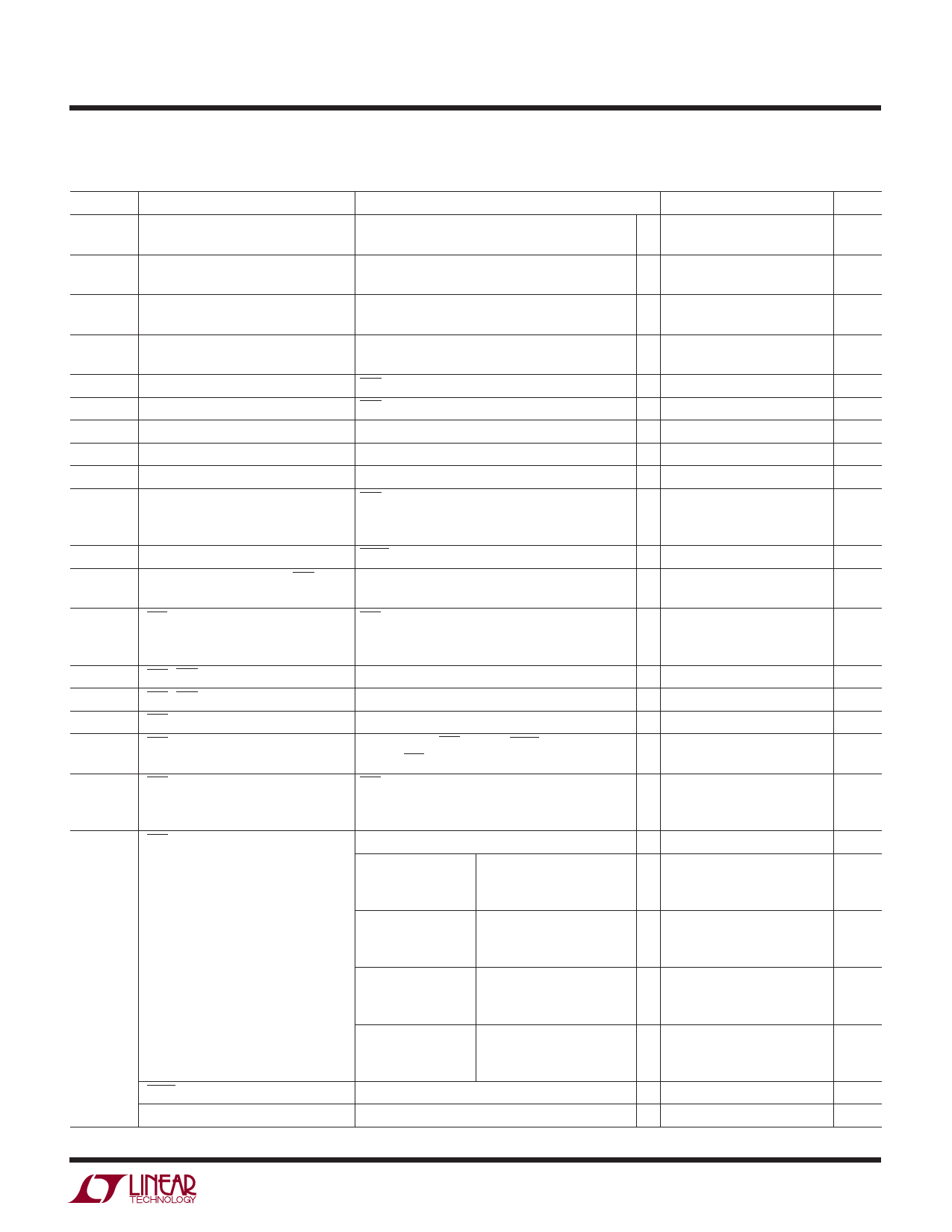
LTC1326/LTC1326-2.5
ELECTRICAL CHARACTERISTICS The ● denotes the specifications which apply over the full operating
temperature range, otherwise specifications are at TA = 25°C. VCC3 = 3.3V, VCC5 = 5V (for LTC1326),VCC25 = 2.5V (for LTC1326-2.5),
VCCA = VCC3, TA = 25°C unless otherwise noted.
SYMBOL PARAMETER
CONDITIONS
MIN TYP MAX UNITS
VRT3
VRT5
VRT25
VRTA
VCC
IVCC3
IVCC5
IVCC25
IVCCA
tRST
tSRST
tUV
IPBR
VIL
VIH
tPW
tDB
Reset Threshold VCC3
Reset Threshold VCC5 (LTC1326)
Reset Threshold VCC25 (LTC1326-2.5)
Reset Threshold VCCA
VCC3 Operating Voltage
VCC3 Supply Current
VCC5 Input Current (LTC1326)
VCC25 Input Current (LTC1326-2.5)
VCCA Input Current
Reset Pulse Width
Soft Reset Pulse Width
VCC Undervoltage Detect to RST
PBR Pull-Up Current
PBR, RST Input Low Voltage
0°C ≤ TA ≤ 70°C
–40°C ≤ TA ≤ 85°C
0°C ≤ TA ≤ 70°C
–40°C ≤ TA ≤ 85°C
0°C ≤ TA ≤ 70°C
–40°C ≤ TA ≤ 85°C
0°C ≤ TA ≤ 70°C
–40°C ≤ TA ≤ 85°C
RST in Correct Logic State
PBR = VCC3
VCC5 = 5V
VCC25 = 2.5V
VCCA = 1V
RST Low with 10kΩ Pull-Up to VCC3
0°C ≤ TA ≤ 70°C
–40°C ≤ TA ≤ 85°C
SRST Low with 10kΩ Pull-Up to VCC3
VCC25, VCC3 or VCCA Less Than Reset
Threshold VRT by More Than 1%
PBR = 0V
0°C ≤ TA ≤ 70°C
–40°C ≤ TA ≤ 85°C
PBR, RST Input High Voltage
PBR Min Pulse Width
PBR Debounce
Deassertion of PBR Input to SRST
Output (PBR Pulse Width = 1µs)
● 3.094 3.118 3.135
V
● 3.052 3.118 3.143
V
● 4.687 4.725 4.750
V
● 4.625 4.725 4.762
V
● 2.344 2.363 2.375
V
● 2.312 2.363 2.381
V
● 0.992 1.000 1.007
V
● 0.980 1.000 1.007
V
●
1
7
V
●
20
40
µA
●
4
10
µA
●
2.8
7
µA
● –15
0
15
nA
● 140
200
280
ms
● 140
200
300
ms
●
50
100 200
µs
13
µs
●
3
7
10
µA
●
3
7
15
µA
●
0.8
V
●
2
V
●
40
ns
●
20
35
ms
tPB
PBR Assertion Time for Transition PBR Held Less Than VIL
from Soft to Hard Reset Mode
0°C ≤ TA ≤ 70°C
–40°C ≤ TA ≤ 85°C
● 1.4
2.0
2.8
s
● 1.4
2.0
3.0
s
VOL
RST Output Voltage Low
ISINK = 5mA
●
0.15
0.4
V
ISINK = 100µA,
VCC3 = 1V, VCC5 = 0V
●
0°C ≤ TA ≤ 70°C
VCC3 = 0V, VCC5 = 1V
●
VCC3 = 1V, VCC5 = 1V
●
0.05
0.4
V
0.05
0.4
V
0.05
0.4
V
ISINK = 100µA,
VCC3 = 1.1V, VCC5 = 0V
●
– 40°C ≤ TA ≤ 85°C VCC3 = 0V, VCC5 = 1.1V
●
VCC3 = 1.1V, VCC5 = 1.1V
●
0.05
0.4
V
0.05
0.4
V
0.05
0.4
V
ISINK = 100µA,
VCC3 = 1V, VCC25 = 0V
●
0°C ≤ TA ≤ 70°C
VCC3 = 0V, VCC25 = 1V
●
VCC3 = 1V, VCC25 = 1V
●
0.05
0.4
V
0.05
0.4
V
0.05
0.4
V
ISINK = 100µA,
VCC3 = 1.1V, VCC25 = 0V
●
– 40°C ≤ TA ≤ 85°C VCC3 = 0V, VCC25 = 1.1V
●
VCC3 = 1.1V, VCC25 = 1.1V ●
0.05
0.4
V
0.05
0.4
V
0.05
0.4
V
SRST Output Voltage Low
ISINK = 2.5mA
●
0.15
0.4
V
RST Output Voltage Low
ISINK = 2.5mA
●
0.15
0.4
V
132625fc
3
Share Link: 