LTC1326 View Datasheet(PDF) - Linear Technology
Part Name
Description
Manufacturer
LTC1326 Datasheet PDF : 16 Pages
| |||
LTC1326/LTC1326-2.5
WU
W
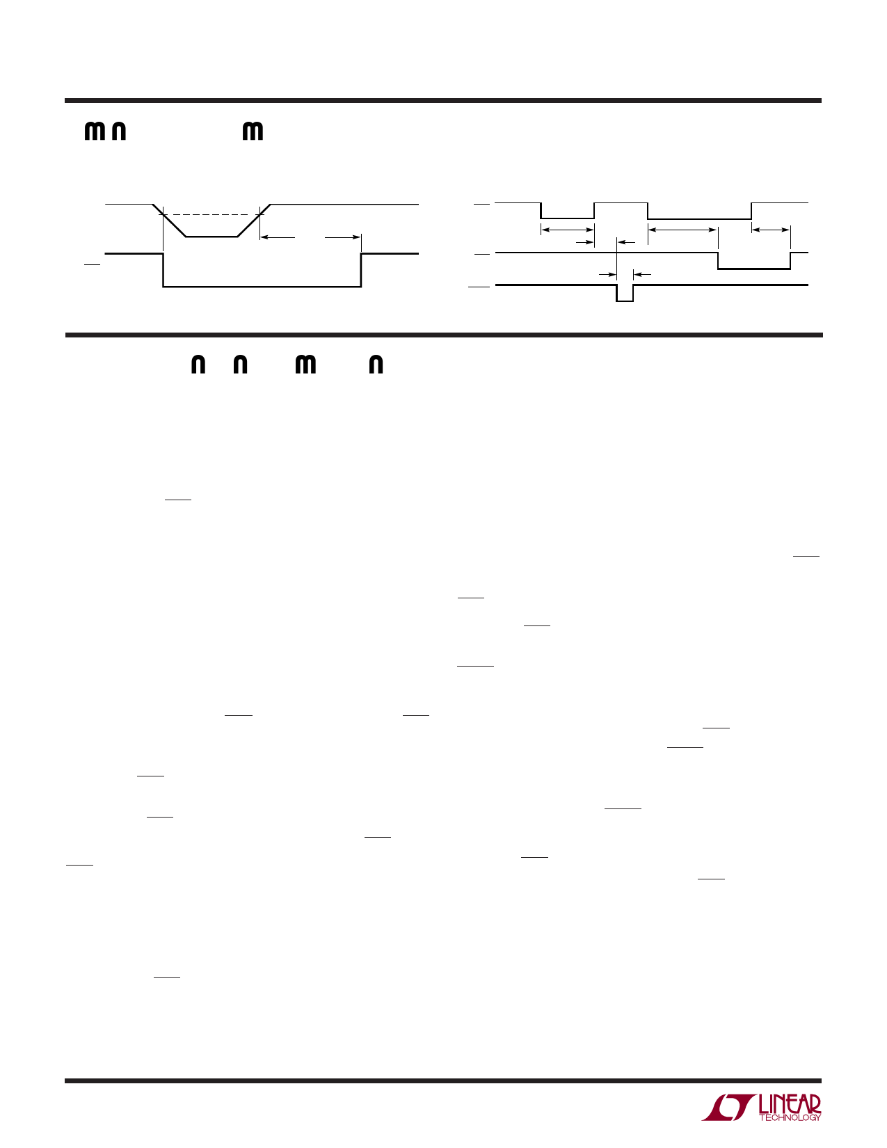
TI I G DIAGRA S
VCC Monitor Timing
VCCX
VRTX
tRST
RST
1326/2.5 TD01
Push-Button Reset Function Timing
PBR
t < tPB
tPB
tRST
tDB
RST
tSRST
SRST
1326/2.5 TD02
APPLICATIO S I FOR ATIO
Operation
The LTC1326/LTC1326-2.5 are micropower, high accu-
racy triple supply monitoring circuits. The parts have two
basic functions: generation of a reset when power sup-
plies are out of range, and generation of reset or a “soft”
reset when the PBR pin is pulled low.
Supply Monitoring
All three VCC inputs must be above predetermined
thresholds for 200ms before the reset output is released.
The parts will assert reset during power-up, power-down
and brownout conditions on any one or more of the VCC
inputs.
On power-up, either the VCC5 or VCC3 pin on the LTC1326,
or the VCC25 or VCC3 pin on the LTC1326-2.5, can power
the drive circuits for the RST pin. This ensures that RST
will be low when VCC5, VCC25 or VCC3 reaches 1V. As long
as any one of the VCC inputs is below its predetermined
threshold, RST will stay a logic low. Once all of the VCC
inputs rise above their thresholds, an internal timer is
started and RST is released after 200ms. The RST pin
outputs the inverted state of what is seen on RST pin.
RST is reasserted whenever any one of the VCC inputs
drops below its predetermined threshold and remains
asserted until 200ms after all of the VCC inputs are above
their thresholds.
On power-down, once any of the VCC inputs drop below
its threshold, RST is held at a logic low. A logic low of 0.4V
is guaranteed until VCC3 and VCC5 on the LTC1326 or VCC3
and VCC25 on the LTC1326-2.5 drop below 1V.
The three internal precision voltage comparators have
response times that are typically 13µs. This slow re-
sponse time helps prevent mistriggering due to tran-
sients on each of the VCC inputs. The part’s ability to
suppress transients can be improved by bypassing each
of the VCC inputs with a 0.1µF capacitor to ground.
Push-Button Reset
The parts provide a push-button reset input pin. The PBR
input has an internal pull-up current source to VCC3. If the
PBR pin is not used it can be left floating.
When the PBR is pulled low for less than tPB (≈ 2 sec), a
narrow (100µs typ) soft reset pulse is generated on the
SRST output pin after the button is released. The push-
button circuitry contains an internal debounce counter
which delays the output of the soft reset pulse by typically
20ms. This pin can be OR-tied to the RST pin and issue
what is called a “soft” reset. The SRST thereby resets the
microprocessor without interrupting the DRAM refresh
cycle. In this manner DRAM information remains undis-
turbed. Alternatively, SRST may be monitored by the
processor to initiate a software-controlled reset.
When the PBR pin is held low for longer than tPB (≈ 2 sec),
a standard reset is generated on the RST and RST pins.
Once the 2 second period has elapsed, a reset signal is
produced by the push-button logic, thereby clearing the
reset counter. Once the button is released, the reset
counter begins counting the reset period (200ms nomi-
nal). Consequently, the reset outputs remain asserted for
approximately 200ms after the button is released.
132625fc
8
Share Link: 